Gerd Binnig and Heinrich Rohrer of the IBM Research Laboratory in Rüschlikon, Switzerland, constructed the first scanning tunneling microscope (STM) in 1981, making individual atoms clearly visible to a select number of specialists for the first time. In 1986, they were awarded the Nobel Prize in Physics. Nanosurf took it a step further in 1997, bringing single atoms into the classroom!
The NaioSTM is a scanning tunneling microscope that combines the scan head and controller into a single instrument for much easier installation, operation and transportability. The system is vibration-resistant and may be utilized in regular classroom settings to attain atomic resolution on HOPG. With a footprint of 204 × 204 mm, it takes up very minimal space.
- Atomic resolution in 5 minutes
- Tiny footprint, easy to store and transport
- Small mechanical loop offers outstanding stability
Smart Design
The system includes a scan head, controller, air-flow shielding with a magnifying glass to facilitate the first approach and vibration isolation on a huge stone table, which is well-suited to the demands of educational institutions.
On a coffee table or in a classroom, the very small mechanical loop of <10 mm offers the stability needed to reach atomic resolution. The extra passive vibration isolation feet further protect measurements from disruptions, resulting in a very robust system when in use. The system does not require high voltage to operate, making it safe in the hands of untrained people.
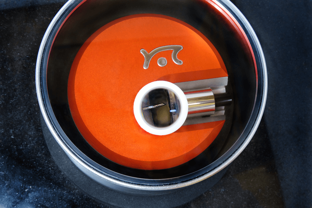
NaioSTM with airflow shielding. The magnifying glass helps with the initial approach.
Image Credit: Nanosurf AG

NaioSTM on heavy stone table: simple and robust setup and measurements.
Image Credit: Nanosurf AG
Ease of Use
The NaioSTM’s innovative design not only provides excellent performance but also makes it incredibly simple to operate. In terms of setup, the user only needs to connect two cables: power and USB. Due to the lack of high voltage and its overall strong construction, it is safe to be handled by students or other users with no prior training.
Scanning tips are simply cut from Pt/lr wire and do not require any dangerous agents to etch. The entire procedure, from setting up to viewing the first good pictures, takes only a few minutes. The user-friendly program includes instructions to assist users with the measuring procedure.
NaioSTM Overview and Tutorial
Nanosurf’s all-in-one scanning tunneling microscope for small samples and nanoeducation is set up and ready for measurement within minutes. Watch this new video and see how easy it is to carry out your first measurement on HOPG. Learn how to cut your own tips from Pt/Ir wire and how to cleave your HOPG sample. Video Credit: Nanosurf AG
The Number One STM Solution in the Field

Left to right: Easyscan STM, Easyscan 2 STM, NaioSTM.
Image Credit: Nanosurf AG
Nanosurf’s scanning tunneling microscope has risen to the top of the field after more than two decades and three generations of development. With around 1500 instruments in use across the world, it is widely considered as the obvious choice for performing scanning tunneling microscopy in all sorts of educational settings and fundamental research due to its smart construction.
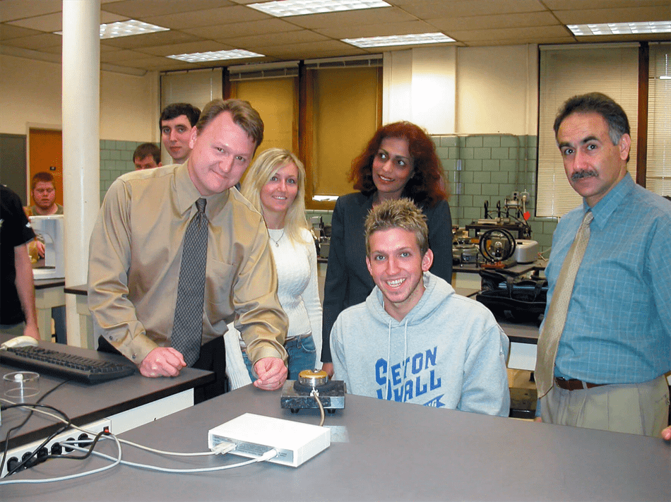
The 500thEasyscan STM is taken into operation.
Image Credit: Nanosurf AG
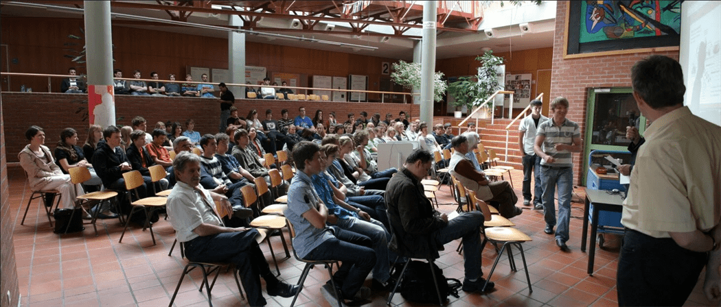
The 1000thSTM microscope was installed at the Claude-Dornier-Schule in Friedrichshafen, Germany.
Image Credit: Nanosurf AG
Professors and teachers like carrying out practical demonstrations on the NaioSTM as it is simple to use, and students find it incredibly motivating to be able to effectively complete hands-on experiments without extensive preparation.
Scanning tunneling microscopy is regarded as one of nanotechnology’s cornerstones. Nanosurf, when used in conjunction with the NaioAFM, brings atomic-scale nanotechnology to the classroom, bringing insights into biology, chemistry and physics.
Why is this STM so Popular in the Classroom?
- Teachers are satisfied with how simple Nanosurf STMs operate, since it allows them to give their students rapid and easy demonstrations in the classroom.
- Students are inspired by the quick results they get while utilizing the STMs during hands-on instruction.
- Because the conducting tips are simply cut from Pt/Ir wire and do not need etching in toxic solvents, anybody may safely use a Nanosurf STM.
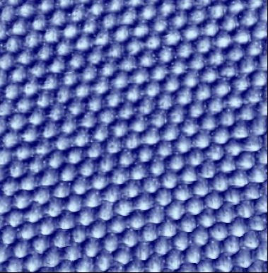
STM image of an atomic lattice, HOPG.
Image Credit: Nanosurf AG
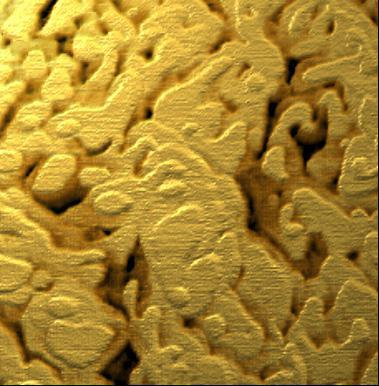
STM image, step height, gold.
Image Credit: Nanosurf AG

Quantum mechanics, charge density.
Image Credit: Nanosurf AG
NaioSTM Imaging Modes
This diagram depicts the instrument’s many modes. Some modes may involve the use of extra hardware or software. Please see the brochure for further information or contact directly.
Imaging Modes
- Constant height (current)
- Constant current (topography)
Spectroscopy Modes
- Current-distance
- Current-voltage
Lithography Modes
System Specifications
NaioSTM Specifications. Source: Nanosurf AG
| . |
. |
| Max. scan range (XYZ)(1) |
500 nm x 500 nm x 200 nm |
| Scan resolution (XYZ) (2) |
7.6 pm × 7.6 pm × 3.1 pm |
| Current amplifier |
0.1–100 nA in 25 pA steps |
| Sample approach |
Stick-slip motor |
| Sample size |
Max. 10 mm diameter, Max. 3 mm thickness |
| Data points |
Imaging: up to 2048×2048, Spectroscopy: up to 65535 |
| Imaging speed |
Up to 10 Hz |
| Computer requirements |
USB 2.0, Windows 7 or higher (32- or 64-bit)/td> |
| Power supply |
90–240 V AC, 50/60 Hz, 30 W |
| Size (WDH), Weight |
204 × 204 × 104 mm, 3.45 kg |
(1) Typical values.
(2) Calculated by dividing the maximum range by 16 bits.
System Dimensions
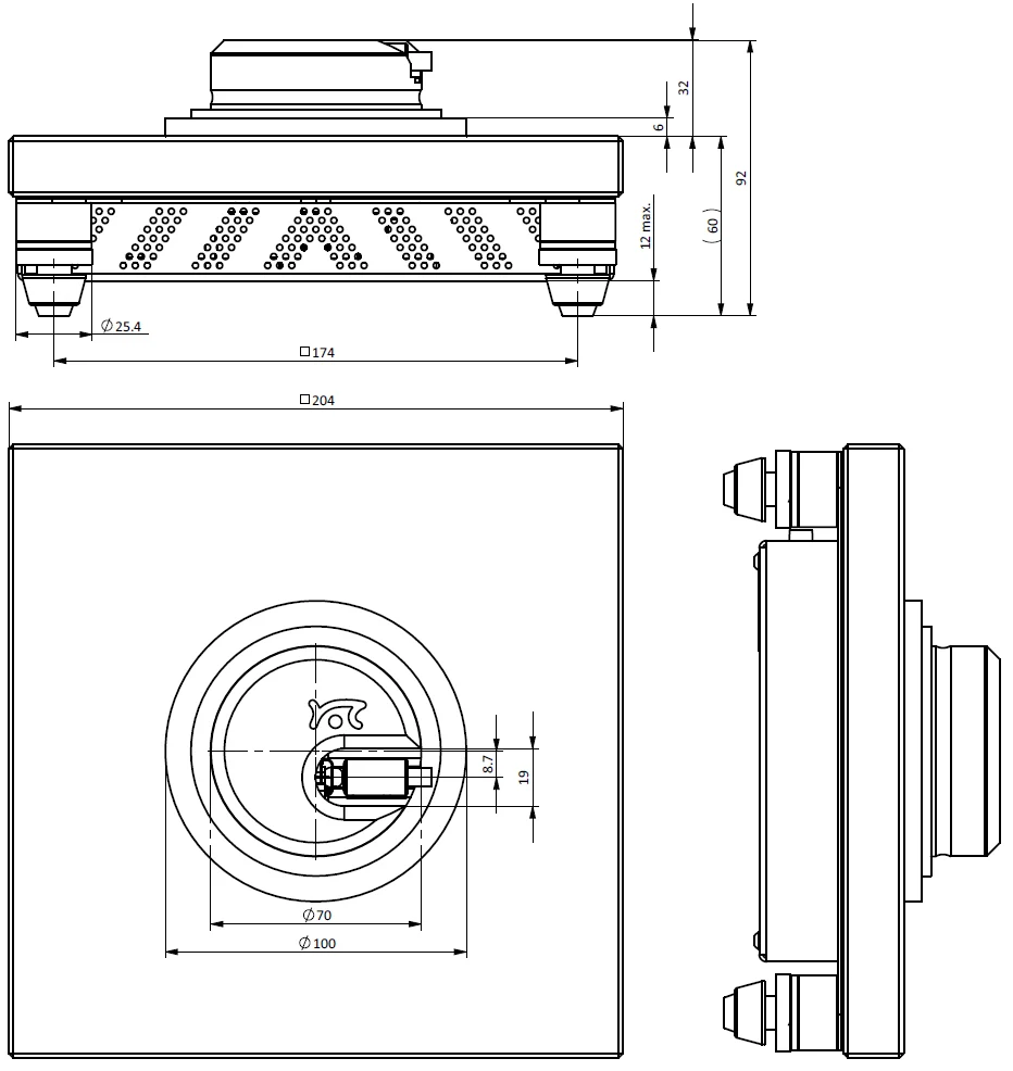
Image Credit: Nanosurf AG