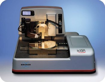
Bruker today announced the release of the Photoconductive Atomic Force Microscopy (pcAFM) module for its industry leading Dimension Icon platform.
 Bruker's Dimension Icon Atomic Force Microscope
The new accessory enables sample illumination while performing nanoscale electrical characterization. In conjunction with Bruker's exclusive PeakForce TUNA technology, it uniquely enables highest resolution photoconductivity and correlated nanomechanical mapping for research on fragile organic light emitting diode (OLED) and organic photovoltaic (OPV) device samples. The pcAFM module is compatible with Bruker's turnkey 1ppm glove box configuration, addressing the most stringent environmental control needs of organic photoelectric materials.
"Organic photoelectric materials are already finding large markets as OLEDs in mobile device displays. There is also interesting research being conducted on OPV devices," said Mark R. Munch, Ph.D., President of Bruker Nano Surfaces Division. "Our new pcAFM accessory transforms the Dimension Icon AFM into a solution for dedicated nanoscale organic photoelectric material research."
"Nanoscale structure and properties are at the core of key OLED and OPV performance parameters," added David V. Rossi, Executive Vice President and General Manager of Bruker's AFM Business. "Our new pcAFM module builds on our exclusive PeakForce Tapping technology to provide the best, highest resolution data advancing organic photoelectric material research."
About the Dimension Icon Photoconductive AFM Module
The Dimension Icon pcAFM accessory is a modular addition to the Dimension Icon platform designed to retain the system's top levels of performance while enabling photoconductivity measurements on OLEDs, OPVs and other photoelectric materials. It provides uniform backside sample illumination and can be fiber coupled to industry-standard solar simulators. In combination with Bruker's exclusive PeakForce TUNA, it addresses the key challenge to avoid sample damage on fragile OLED and OPV samples, thus retaining highest spatial resolution photoconductivity data. It is fully compatible with Bruker's turnkey 1ppm glove box configuration, guaranteeing that measurements are not compromised by environmental material degradation.