.jpg)
Dr Mark Munch, President of Bruker Nano Surfaces, talks to AZoNano about the challenges and opportunities for AFM research at the Seeing at the Nanoscale event in Bristol.
So Mark, it's been nearly a year and a half since the transition from Veeco Metrology to Bruker Nano Surfaces, and I'm sure there have been many changes during that process. What are the key changes you have seen?
Well they've been really positive changes - it's been a smooth transition. We really found a better home with Bruker, because they're a scientific instrument company, which is a better fit for us.
We've seen enhanced investment in our sales coverage, in our service coverage, in our facilities - we've upgraded our facilities around the world, we've upgraded our factories - and we've had a lot of tremendous support for partnerships, and for acquisitions. In fact, just recently, at the end of last year, we completed an acquisition in Campbell California, the acquisition of CTR.
So it's been a very, very supportive environment - those have been the four areas of really positive change for us. And we've done all that, integrating into Bruker, without slowing down in innovation at all. We've put out a number of products, just as we did under Veeco. That rate of innovation has just continued under Bruker.
Interview with Dr Mark Munch, President of Bruker Nano Surfaces
What would you see as the key challenges in the near future to more widespread AFM adoption?
These have really been long-standing challenges for the whole AFM industry, in terms of adoption.
Ease of use - traditionally AFMs are known to be very hard to use, you have to be very specialized in order to get really high quality, good results. So we've been focusing on ease of use, and you see that manifested by the invention of Peak Force Tapping Mode, and within that mode we offer ScanAsyst. So you find Icon with ScanAsyst, Multimode with ScanAsyst, BioScope Catalyst with ScanAsyst. So ease of use is very important, and we've been charging down that path, leading the way for the industry.
In addition to that, faster imaging. To take a really high quality image, traditionally you have to be very patient. We've changed the game in that, allowing image acquisition speed 100 times faster.
Also - whilst increasing ease of use, and faster scanning at the same time - increasing performance range. Going down to softer materials without sample damage, and really broadening the applications.
These have been major challenges, and I think we've been making really good progress around all three fronts, it's been going very well.

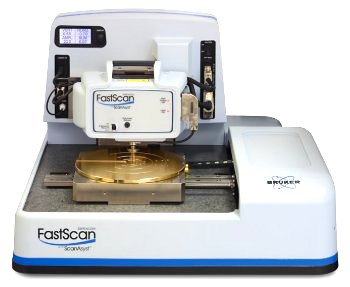
Bruker's Dimension FastScan AFM images hundreds of times faster without loss of resolution.
So with all these advances, what direction do you see nanoscience research going and developing, using these AFM techniques?
So in addition to ease of use and fast imaging, and everything I just talked about, going beyond topography is really key. So we are providing fast topography, and ease of use towards topography, but also providing quantitative nanoscale information, such as quantitative nanomechanical information, quantitative nanoelectrical information, quantitative chemical ID.
Because scientists want to understand - you give me a really interesting picture of the surface, really interesting topography, now tell me more about "what is it?" What is it mechanically, electrically, what is it chemically? So these are really important research directions that we are also investing in.
What would you say are the key advantages that Bruker AFM systems offer over other competitors in the field?
Well, of course I'm biased in my answer to this! But I do really think that we lead the way in breadth of products to suit any application. We have the largest offering in products, and the largest offering in modes. We have a very complete set of products and mode sets - electrical modes, topography modes, mechanical modes.
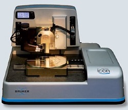
In addition to that, we really have led the way in terms of instrument stability for large scanning. Dimension Icon is a very stable platform - we've been able to achieve atomic scale resolution over large scans. That's a first from the industry - to be able to scan at that range, and image with atomic scale resolution. And furthermore, doing that while going fast. Our Dimension FastScan also images atomic scale over large scan lengths.
So there are a number of advantages that we have that we're very, very proud of. I think our development teams and research teams have done a great job leading the way. And that's going to help the industry, because what we do to help our customers really helps push the whole industry forward.

The Dimension Icon AFM from Bruker delivers revolutionary low drift and low noise over a 90µm scan range.
Seeing at the Nanoscale is clearly a hugely popular event in the AFM community. What are your plans for the event next year?
Seeing at the Nanoscale is a key event, because it really facilitates technical exchange, and brings the industry together to exchange ideas. And we've selected some very nice locations, such as Bristol, to do that.
We're really going to enhance the number of collaborations we have, leverage the "Seeing" brand, because we've built quite a brand for the event, and I think it's really important that we leverage that by building on the number of collaborations, by doing more "Seeing" events, but also increasing the geographic reach.
We often go back to Santa Barbara, for example, for every other Seeing at the Nanoscale. So we're going to explore other geographies, and you'll see us not just bouncing back and forth between the US and Europe, but actually going to other regions of the world. So because we've built this brand, and because it's a really effective conference, why not leverage it more broadly?
Thanks a lot Mark, good luck with the expansion of the event next year, and all these developments in the future.
You're welcome, nice to meet you.
About Bruker Nano Surfaces
Bruker Nano provides Atomic Force Microscope/Scanning Probe Microscope (AFM/SPM) products that stand out from other commercially available systems for their robust design and ease-of-use, whilst maintaining the highest resolution. Click here for more information on Bruker Nano Surfaces.

Disclaimer: The views expressed here are those of the interviewee and do not necessarily represent the views of AZoM.com Limited (T/A) AZoNetwork, the owner and operator of this website. This disclaimer forms part of the Terms and Conditions of use of this website.