Scanning Capacitance Microscopy (SCM) and Scanning Spreading Resistance Microscopy (SSRM) are both established scanning probe-based techniques for two-dimensional carrier profiling.
It was mainly the microelectronics industry that pushed their initial development by looking for 2D alternatives for their 1D carrier/dopant profiling methods, like Secondary Ion Mass Spectrometry (SIMS), Capacitance-Voltage (C-V) measurements, and Scanning Resistance Profiling (SRP).
In SSRM, the resistance of the current spreading through the nanoscale tip-sample contact is quantified while scanning the probe. The key to its large sensitivity and spatial resolution is in the presence of a pressure-induced metallic pocket below the tip apex leading to an almost ohmic tip-sample contact.
The measured resistance is dominated by the spreading resistance and so, dependent on the local sample resistivity ρ as a result of this:
Rspreading = ρ/4a,
Where a represents the contact size. The key benefits of SSRM include a large sensitivity and dynamic range (1014-1020 cm-3) and an extremely high spatial resolution (~ 1 nm). Small capacitance variations (~10-21 F) between the tip and the sample are measured in SCM, by utilizing a high-frequency capacitance sensor while scanning the probe.
Lowly doped areas exhibit a relatively larger capacitance change, while highly doped regions show a low differential capacitance dC/dV. The main benefits are the carrier type sensitivity and the large dynamic range as n- and p-type show opposite phases in their dC/dV signals.
In both techniques, it is not easy to convert the measured values directly into quantitative values for carriers as detailed information on the probe and sample surface are absent.
So usually, a calibration against a known standard is the easiest way to convert resistance/differential capacitance to resistivity/carrier concentrations. In fact, both methods have benefits and drawbacks, but are quite complementary; SCM supplies carrier type sensitivity, while SSRM supplies the highest spatial resolution.
The requirements for materials and device characterization are being pushed to their limits as current state-of-the-art devices are entering the sub 10 nm nodes, needing each part of the measurement to be optimized for successful measurements, for instance, the sample preparation, the probe, and the measurement environment.
In this article, the performance of the Park NX-Hivac atomic force microscope (AFM) from Park Systems1 for SSRM and SCM applications is assessed, based on the following three samples:
- An n-type doped silicon calibration sample (imec CS01-SiAs): a sample that is made up of a number of arsenic doped epitaxial silicon layers with known doping concentration (Figure 5). This sample also has a p-type doped layer embedded in the stack.
- Buried oxide sample: a 0.5 nm oxide layer sandwiched in between a highly doped Si and a poly-Si layer (Figure 2).
- A p-type doped silicon calibration sample (imec CS08-SiB): a sample made up of various Boron doped epitaxial silicon layers (~600 nm) with known doping concentration (Figure 1).
These samples are quantified on the Park NX-Hivac AFM system, operating in vacuum conditions (~5e-5 mbar) utilizing imec Full Diamond probes2.
SSRM – Basic Performance
Firstly, to investigate the repeatability of SSRM measurements, the p-type calibration sample is measured. Figure 1 demonstrates that excellent repeatability is acquired in SSRM measurements on silicon.
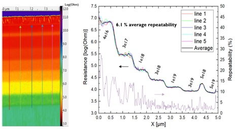
Figure 1. SSRM measurement on a p-type doped silicon calibration sample performed in a vacuum. The colored resistance cross-sections are taken from single line scans and the black line is the average over those 5 scan lines. The repeatability is plotted in purple (right Y-axis).
It is worth noting that in the highly doped layers, the repeatability is better. As an example, for identical scanning parameters, usually repeatability of 15-20 % is acquired in air highlighting the added value of high vacuum3.
Next, the buried oxide sample is measured to examine the resolution of SSRM. Figure 2 shows that the 0.5 nm oxide layer embedded in silicon can be seen easily in SSRM measurements as an increase in the resistance.
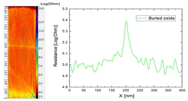
Figure 2.: High-resolution SSRM measurement on a 0.5 nm oxide layer sandwiched in between highly doped Si and poly-Si layers. The resistance cross-section is taken from a single scan line.
The doubling of the resistance on the thin oxide demonstrates that the electrical contact radius is similar to the oxide thickness, highlighting a sub-nm resolution2. Lastly, to verify the advantages of performing SSRM measurements in a vacuum environment, the p-type calibration sample is measured in air and in a vacuum with the same probe.
Figure 3 summarizes the results. As predicted, the applied force to the tip needed for a good electrical tip-sample contact had to be increased by nearly 50 % when moving from vacuum to ambient environment to gather an image of similar quality.
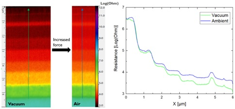
Figure 3. SSRM measurements on a p-type doped silicon calibration sample performed in vacuum and in the air with the same probe. The resistance cross-sections are the average over 50 scan lines.
This observation indicates that the metallic pocket below the tip apex is induced at lower pressure in a vacuum as compared to in the air. So, measurements in a vacuum environment may be carried out with a lower force applied to the tip which will lead to less tip wear and so, higher resolution2.
From the results discussed above it can be concluded that the repeatability and resolution of SSRM measurements carried out on the Park NX-Hivac AFM are state-of-the-art and that the vacuum conditions in the chamber are advantageous for performing repeatable SSRM experiments.
SSRM – Device Measurements and Calibration
Generally, the calibration samples enable the conversion of the resistance map of an unknown sample to a carrier concentration map. To achieve this, the calibration sample is measured with the same probe and scan parameters as the measurement on the sample of interest.
In Figure 4 for example, the resistance and carrier concentration maps of an n-type doped silicon layer in a solar cell can be observed. By utilizing the calibration curve that is shown in Figure 5, the carrier concentration map is calculated from the resistance map.
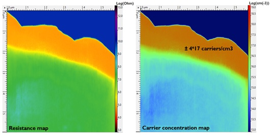
Figure 4. SSRM resistance and carrier concentration maps of an n-type doped silicon layer in a solar cell sample.
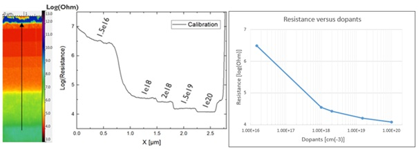
Figure 5. SSRM measurement on an n-type doped silicon calibration sample. The resistance cross-section is taken from an average of 50 scan lines. The resistance versus dopants data points is taken from the average resistance values measured over the 5 layers with known doping levels in the calibration sample.
The resistance data points are taken from the average resistance values measured over the five layers with known doping levels. The calibration curve is then acquired by the interpolation of these data points.
It can be concluded that in a sample with unknown carrier levels, the good measurement repeatability on both the sample and the standard enables an accurate determination of the active carrier concentration.
SCM
In order to evaluate the performance of SCM on the Park NX-Hivac AFM, The n-type doped silicon calibration sample is used. Next to the n-type epitaxial layers, this sample also has a p-type doped layer in between the substrate and the n-layers.
The dC/dV amplitude and the dC/dV phase map gathered from an SCM measurement on the n-type calibration sample are shown in Figure 6. It is possible to clearly distinguish the n and p-layers from the phase map.
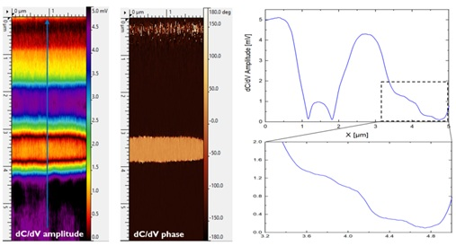
Figure 6: SCM dC/dV amplitude and phase measurements on an n-type doped silicon calibration sample. The dC/dVamplitude cross-section is taken from an average of 50 scan lines.
The numerous n-type layers with different doping concentrations also show a clear contrast in the dC/dV amplitude map. Even though the spatial resolution is not as good as in SSRM, these results exhibit the carrier concentration sensitivity and the carrier type sensing capability of SCM.
Other than Si, another interesting application of SCM is on III-V material stacks. The results of an SCM measurement on a doped InGaAs stack can be seen in Figure 7, and they enable the extraction of information about the carrier type and the carrier concentration.
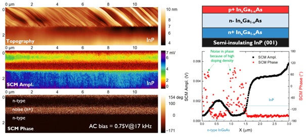
Figure 7: SCM measurement on a doped InGaAs stack. The dC/dV amplitude and phase cross-sections are taken from the average of 100 scan lines.
Conclusions
This study shows that with the right microscopy tool, scanning capacitance microscopy (SCM) and scanning spreading resistance microscopy (SSRM) can meet the challenges of carrier profiling the state-of-the-art devices entering the sub 10 nm nodes.
This study found that Park NX-Hivac is a powerful tool that meets the challenges of ever-shrinking devices with its implementation of electrical SPM modes in a high vacuum environment, including SSRM and SCM.
In addition, this article demonstrates that the utilization of Park NX-Hivac vacuum helps significantly to decrease the noise, leading to average repeatability of 6.1 % for SSRM measurements.
References and Further Reading
- Park NX-Hivac, Retrieved from https://www.parksystems.com/en/products/research-afm/specialized-afm/nx-hivac
- Hantschel, T., et al. Diamond scanning probes with sub-nanometer resolution for advanced nanoelectronics device characterization, Microelectronic Engineering 159, 46-50 (2016).
- Eyben, P. et al. Fundamentals of Picoscience, Subnanometer Characterization of Nanoelectronic devices. Edited by Sattler, K.D., CRC Press (2014)
Acknowledgments
Produced from materials originally authored by Lennaert Wouters1, Albert Minj1,2, Umberto Celano1, Thomas Hantschel1, Wilfried Vandervorst1,2, and Kristof Paredis1 from
- IMEC, Leuven, Belgium
- Department of Physics and Astronomy, University of Leuven, Leuven, Belgium

This information has been sourced, reviewed and adapted from materials provided by Park Systems.
For more information on this source, please visit Park Systems.