Feb 17 2017
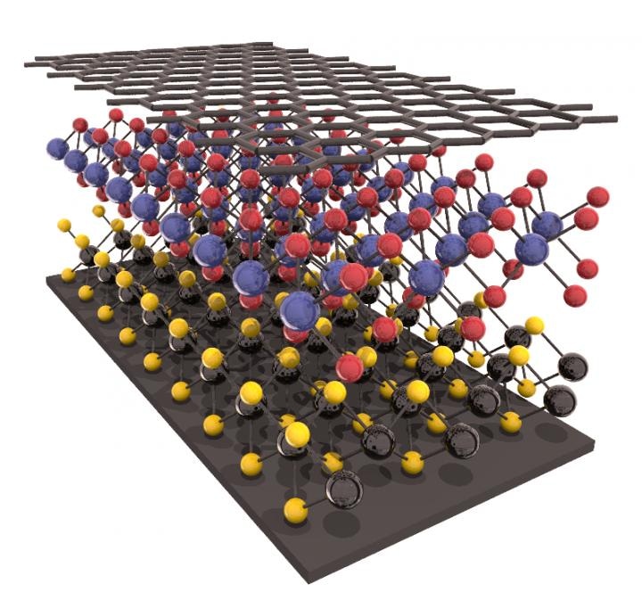
 This is a heterostructure of two-dimensional 'wonder' materials. (Credit - Gabriel Constantinescu)
Dr Neil Wilson in the Department of Physics at the University of Warwick has developed a new method to measure the electronic structures of stacks of two-dimensional (2D) materials – flat, atomically thin, extremely strong, and highly conductive materials – for the first time.
Heterostructures, typically multiple stacked layers of 2D materials, create highly efficient optoelectronic devices with ultrafast electrical charge, which can be applied in nano-circuits, and are more robust than materials used in traditional circuits.
A number of heterostructures have been designed using different 2D materials – and stacking a variety of combinations of 2D materials creates new materials possessing new properties.
The electronic properties of each layer in a stack are measured by Dr Wilson’s method, allowing researchers to determine the most favorable structure to transfer electrical energy in the fastest and most efficient manner.
The method uses the photoelectric effect to immediately measure the momentum of electrons within each layer, and reveals how this transforms when the layers are combined.
The ability to understand and compute the way 2D material heterostructures function, and to form optimal semiconductor structures – opens the door for the development of highly efficient nano-circuitry, and flexible, smaller, and more wearable devices.
Solar power could also be transformed using heterostructures, as the atomically thin layers are ideal for strong absorption and efficient power conversion using small quantity of photovoltaic material.
It is extremely exciting to be able to see, for the first time, how interactions between atomically thin layers change their electronic structure. This work also demonstrates the importance of an international approach to research; we would not have been able to achieve this outcome without our colleagues in the USA and Italy.
Dr Neil Wilson, University of Warwick
Dr Wilson developed the method with colleagues in the theory groups at the University of Warwick and University of Cambridge, at the University of Washington in Seattle, and the Elettra Light Source, near Trieste in Italy.
Computational models built by Dr Nick Hine, also from Warwick’s Department of Physics helped to understand how interactions between the atomic layers transformed their electronic structure.
The research paper titled, ‘Determination of band offsets, hybridization, and exciton binding in 2D semiconductor heterostructures’, is published in Science Advances.