May 23 2017
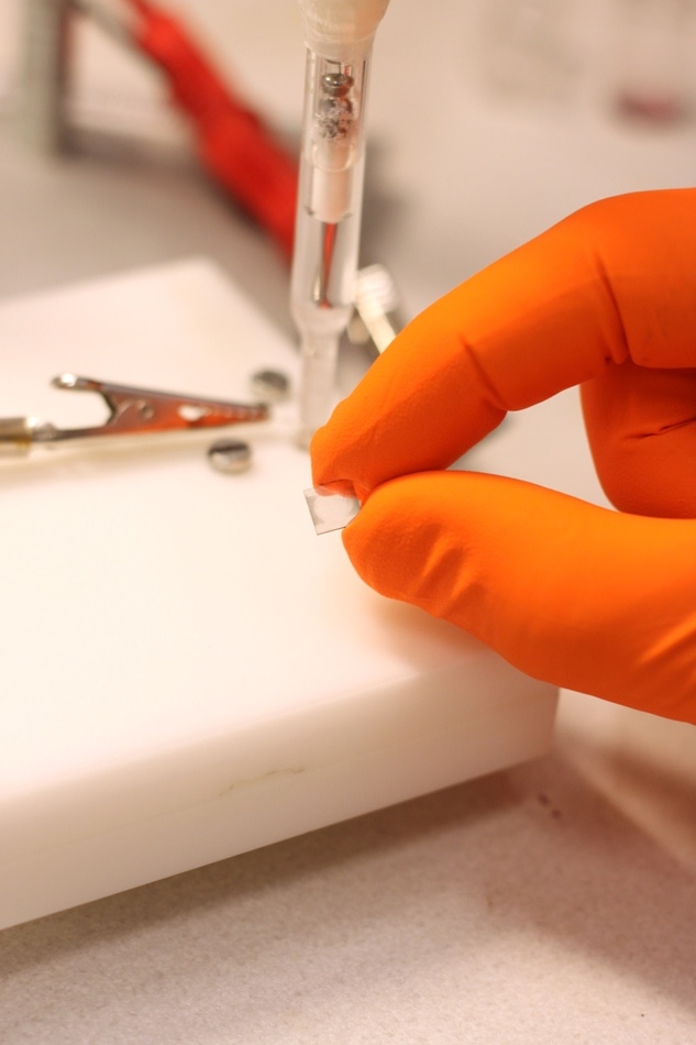
 Researchers at Linkoping University, Sweden, studied graphene on silicon carbide. Photo: Karin Soderlund Leifler
Researchers at Linköping University in Sweden introduced defects into the perfect surface of graphene on silicon carbide in order to increase the material’s capacity to store electrical charge. A report on this has been featured in the scientific journal Electrochimica Acta. This report increases the understanding of how this ultrathin material can be used.
Graphene, the thinnest material ever produced, comprises of a single layer of carbon atoms. They produce a chicken-wire structure one atom thick, with exceptional properties. Besides being flexible, graphene is almost 200 times stronger than steel. Liquids and gases cannot pass through it even though it is transparent. Graphene is also considered to be an exceptional conductor of electricity. A number of ideas are available on how to use this nanomaterial, and research on the future use of this material is rapidly growing.
Graphene is fascinating, but extremely difficult to study.
Mikhail Vagin, Principal Research Engineer, Department of Science and Technology, Linköping University
One factor that makes understanding of the properties of graphene a difficult process refers to fact that graphene is known as an “anisotropic” material. This explains that its properties differ from those measured at the edges when they are measured on the plane surface of the carbon atom layer. The fact that graphene can be produced in several ways actually complicates the attempts to understand the behavior of graphene at the atomic level. The properties of graphene in small flakes, which have several edges, vary in a number of ways from those of graphene developed as sheets with an area around 1 cm2.
The researchers who executed the study used graphene produced on a crystal of silicon carbide by a method created at Linköping University. Silicon atoms on the surface travel to the vapor phase leaving behind only the carbon atoms when silicon carbide is heated to 2000 °C. The high quality of the graphene layer and its innate inertness prevent the graphene from reacting easily with its surroundings, while applications mostly depend on controlled interaction between material and the surroundings, such as gas molecules. Researchers in the field are constantly discussing the possibility of activating the graphene on the flat surface or whether it is actually essential to have edges. The researchers from LiU have examined what happens when defects in the surface are launched in a controlled manner, and this has improved their understanding of how the properties of graphene are linked to its structure.
An electrochemical process known as ‘anodising’ breaks down the graphene layer such that more edges are created. We measured the properties of anodised graphene and discovered that the capacity of the material to store electricity was quite high.
Mikhail Vagin, Principal Research Engineer, Department of Science and Technology, Linköping University
More work is required before using the new knowledge, and also to produce the same effect at a bigger scale. The scientists plan to follow up the research in a number of ways.
Graphene on silicon carbide can be made in larger areas than other types of graphene. If we can change the properties of the material in a controlled manner, it may be possible to tailor the surface for other functions. It may be possible, for example, to create a sensor that has its own built-in battery.
Mikael Syväjärvi, Chief Research Engineer, Department of Physics, Chemistry and Biology, Linköping University
The results were the outcome of a degree project carried out as a teamwork between Graphensic and researchers at Linköping University.