Oct 15 2009
Arradiance, Inc. announced today the demonstration of the world's highest gain microchannel plate, with measured gain reaching 1 million at selected operating parameters.
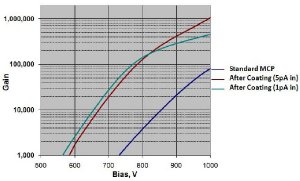
 Performance improvement using GEM-D2 process. (Graphic: Business Wire)
Microchannel plates are used in numerous imaging and detection applications where high spatial and temporal resolution coupled with high signal to noise ratio are important. Example applications include: space science, biotechnology, analytical instrumentation, homeland security and night vision.
“For decades, microchannel plate performance has improved only marginally due to a manufacturing process which has been constrained by available materials and processes,” explains Neal Sullivan, CTO of Arradiance. “The requisite lead-glass substrate material has limited the ability to optimize microchannel plate performance for applications where lifetime, gain and substrate size or composition are important. Arradiance's proprietary thin film technology now makes it possible to overcoat standard lead-glass MCPs and also to fabricate microchannel plates from many substrate materials, including non-lead containing glasses, ceramics, silicon and even plastic while enabling independent optimization of the functional films used for resistance and for secondary emission yield, which makes it possible to achieve these high gains.”
The high measured gain was demonstrated by applying Arradiance's patent-pending GEM-D2™ thin film dynode process to a standard, commercially available, 60:1, 12 micron pitch, 12° bias angle microchannel plate. As received, the plate showed a typical gain for a plate of this configuration of 70,000 at 1,000 V bias and approximately 6 pA input current. At similar input current and voltage following the GEM-D2™ process, a gain of over 400,000, (>5X improvement) was achieved. At a lower input current (~1pA), the gain exceeded 1 million.
“The conventional way to achieve gain of this order has been to stack MCPs in a chevron pattern, thus getting a multiplicative effect. But, stacking MCPs for high gain has always been challenging,” explains David Beaulieu, Arradiance Chief Operating Officer. “Matching resistance and finding the proper alignment to optimize spatial resolution makes the process difficult and expensive. Using the GEM-D2 process can eliminate these issues.”