Feb 12 2010
Material scientists at the Nano/Bio Interface Center of the University of Pennsylvania have demonstrated the transduction of optical radiation to electrical current in a molecular circuit. The system, an array of nano-sized molecules of gold, respond to electromagnetic waves by creating surface plasmons that induce and project electrical current across molecules, similar to that of photovoltaic solar cells.
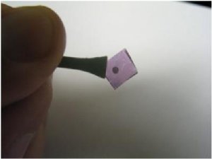
 Material scientists at the Nano/Bio Interface Center of the University of Pennsylvania have demonstrated the transduction of optical radiation to electrical current in a molecular circuit. Credit: Dawn Bonnell, the University of Pennsylvania
The results may provide a technological approach for higher efficiency energy harvesting with a nano-sized circuit that can power itself, potentially through sunlight. Recently, surface plasmons have been engineered into a variety of light-activated devices such as biosensors.
It is also possible that the system could be used for computer data storage. While the traditional computer processor represents data in binary form, either on or off, a computer that used such photovoltaic circuits could store data corresponding to wavelengths of light.
Because molecular compounds exhibit a wide range of optical and electrical properties, the strategies for fabrication, testing and analysis elucidated in this study can form the basis of a new set of devices in which plasmon-controlled electrical properties of single molecules could be designed with wide implications to plasmonic circuits and optoelectronic and energy-harvesting devices.
Dawn Bonnell, a professor of materials science and the director of the Nano/Bio Interface Center at Penn, and colleagues fabricated an array of light sensitive, gold nanoparticles, linking them on a glass substrate. Minimizing the space between the nanoparticles to an optimal distance, researchers used optical radiation to excite conductive electrons, called plasmons, to ride the surface of the gold nanoparticles and focus light to the junction where the molecules are connected. The plasmon effect increases the efficiency of current production in the molecule by a factor of 400 to 2000 percent, which can then be transported through the network to the outside world.
In the case where the optical radiation excites a surface plasmon and the nanoparticles are optimally coupled, a large electromagnetic field is established between the particles and captured by gold nanoparticles. The particles then couple to one another, forming a percolative path across opposing electrodes. The size, shape and separation can be tailored to engineer the region of focused light. When the size, shape and separation of the particles are optimized to produce a "resonant" optical antennae, enhancement factors of thousands might result.
Furthermore, the team demonstrated that the magnitude of the photoconductivity of the plasmon-coupled nanoparticles can be tuned independently of the optical characteristics of the molecule, a result that has significant implications for future nanoscale optoelectronic devices.
"If the efficiency of the system could be scaled up without any additional, unforeseen limitations, we could conceivably manufacture a one-amp, one-volt sample the diameter of a human hair and an inch long," Bonnell said.
The study, published in the current issue of the journal ACS Nano, was conducted by Bonnell, David Conklin and Sanjini Nanayakkara of the Department of Materials Science and Engineering in the School of Engineering and Applied Science at Penn; Tae-Hong Park of the Department of Chemistry in the School of Arts and Sceicnes at Penn; Parag Banerjee of the Department of Materials Science and Engineering at the University of Maryland; and Michael J. Therien of the Department of Chemistry at Duke University.
This work was supported by the Nano/Bio Interface Center, National Science Foundation, the John and Maureen Hendricks Energy Fellowship and the U.S. Department of Energy.