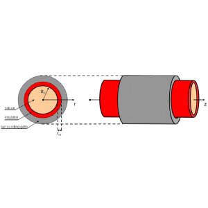
The nanowire pinch-off field effect transistor (FET) or junctionless transistor is a uniformly doped nanowire without junctions with a wrap-around gate. The idea and basic working principle of the nanowire pinch-off transistor were developed in imec and already reported in 2007 and 2008.
Recent modeling results obtained in imec for a GaAs and Si nanowire indicate that the nanowire pinch-off FET can outperform the nanowire MOSFET. These results combined with scalability and ease of processing make the junctionless transistor a true competitor for the nanowire MOSFET.
 Schematic representation of the cylindrical wrap-around gate nanowire
Several years ago, imec theoreticians developed the concept of the pinch-off nanowire FET. Originally, the idea was to avoid surface interactions such as surface roughness scattering or high-k surface phonon scattering wich degrade the charge carrier mobility, by moving the charge carriers away from the interface between the substrate and the insulator. The solution to this problem was to consider a nanowire where source, drain and channel are uniformly doped. For a n-type nanowire pinch-off FET, the charge carriers responsible for the current are delivered by the ionized donors. As the gate voltage is increased, the channel of the wire is depleted and, eventually, pinch-off will occur.
In the nanowire pinch-off FET the charge carriers responsible for the current are occupying the entire volume. As a result, the majority of the carriers do not reside near the interface as is the case in a MOSFET. MOSFET nanowires still require abrupt junctions for their operation and scaling down the channel length more aggressively complicates the fabrication of abrupt junctions. The nanowire pinch-off FET or junctionless transistor is not affected by the aforementioned junction problem which makes the fabrication process much easier. Moreover, simulation results for a GaAs and Si nanowire now show that the nanowire pinch-off FET suffers less from short-channel effects such as drain-induced barrier lowering (DIBL) and subthreshold slope degradation. This makes the nanowire pinch-off FET a true competitor for the nanowire MOSFET for future technology nodes.
More detailed results about the idea and basic working principle of the nanowire pinch-off FET as proposed by imec can be found in:
[1] Sorée, B.; Magnus, W.; Pourtois, G. Analytical and self-consistent quantum mechanical model for a JFET nanowire. In: IWCE12. 2007. (8-10 October 2007; Amherst, NJ, USA.)
[2] Sorée, B.; Magnus, W.; Pourtois, G. Analytical and self-consistent quantum mechanical model for a surrounding gate MOS nanowire operated in JFET mode. JCEL. Vol. 7: (3) 380-383; 2008.