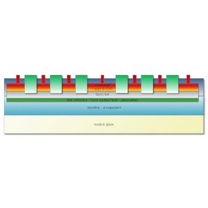
The process that SUGAR proposes resembles a standard thin-film process: deposition on several square meters of amorphous Si, metallization, and laser patterning.
The difference lies in the starting material. Instead of starting from TCO-covered glass, our approach starts from a set of ultra-thin wafers bonded to the glass. Amorphous Si is then deposited and used as a heterojunction emitter. Amorphous-Si emitters have extremely high efficiency potential.
 Scheme of a module-level processed heterojunction cell with inter-digitated back contacts.
Additionally, the SUGAR process will use a combination of heterojunction and inter-digitated back-contact cells, providing an additional potential current increase due to the limited shadowing. Importantly, the process will be achieved on module level and not on wafer level, which is an additional way to reduce volume cost reduction. This means that the metallization step of the inter-digitated back contacted structure is combined with the interconnection of these cells on module level.
The efficiency targets of SUGAR are ambitious but realistic, i.e. a 17% efficiency on module level.
Source: IMEC