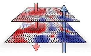
A team at the National Institute of Standards and Technology (NIST) has discovered that electronic traits of two grapheme layers differ on the nano scale.
The results show that not the difference in the electric charges strength between the two layers differ over the layers, but they also reverse in direction to develop random puddles of positive and negative charges. The research paper has been published in Nature Physics, and reveals that the development could help utilize grapheme in consumer electronic devices.
 Graphene layers with insulating substrate causes electrons (red) and electron holes (blue) to collect in puddles
NIST researcher Nikolai Zhitenev says variations in the graphene’s electrical potential could voluntarily cause band gaps due to communication between the graphene electrons or with the substrate the graphene is placed upon.
According to NIST fellow Joseph Stroscio, the measurements show that interactions between random insulating substrate leads to puddles of electrons and electron holes in the graphene layers. Both are of at a greater depth on the lowest layer due to its proximity to the substrate. This difference in pool depths between the layers leads to random alternating charges and the spatially differing band gap. Controlling the substrate purity could allow the team to monitor the band gap and help develop graphene-based transistors that can be switched on or off like a semi-conductor.
Stroscio says that if the substrate communication could be minimized, quantum properties of bilayer graphene could be used to develop a quantum field effect transistor.