Georgia Institute of Technology researchers have described their ‘confinement controlled sublimation’ method for fabricating superior quality large-area layers of epitaxial graphene on silicon carbide wafers in the Early Edition of Proceedings of the National Academy of Sciences journal.
The technique depends on controlling the gas-phase silicon’s vapor pressure in the high-temperature furnace utilized for growing the material. To grow thin graphene layers on silicon carbide, the basic principle is to heat the material to a temperature of 1,500°C under high vacuum. The heat evaporates the silicon, resulting in one or more graphene layers. However, uncontrolled evaporation of silicon results in inferior quality materials that are not suitable for designing electronics devices.
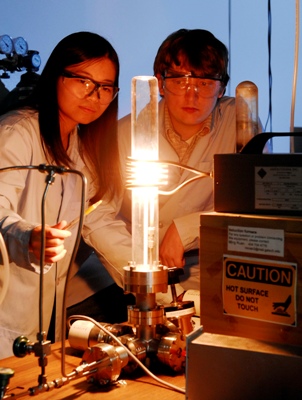
 Georgia Tech graduate students Yike Hu and John Hankinson observe a high temperature furnace used to produce graphene on a silicon carbide wafer. Photo: Gary Meek.
Georgia Tech School of Physics Professor, Walt de Heer, who developed the novel technique, stated that the growth rate of graphene can be controlled by accurately controlling the evaporation rate of silicon, which in turn produces fine epitaxial graphene layers. According to the technique, de Heer's team placed a 1 cm2 silicon carbide wafer in a graphite container. A minute hole in the enclosure controls the release of silicon atoms during the heating process of the wafer by maintaining the rate of condensation and evaporation of silicon near its thermal equilibrium.
The epitaxial graphene fabrication can be performed either in a vacuum or in the presence of an inert gas (argon) and can be utilized to fabricate both single and multiple layers of the wonder material. The paper also elaborates another technique dubbed ‘templated growth’ for the fabrication of narrow graphene ribbons used by de Heer's team.
The templated growth method uses traditional nanolithography techniques to etch patterns into the surfaces of silicon carbide. These patterns act as templates controlling the growth of graphene on parts of the patterned surfaces. This method eliminates the utility of electron beams or other disparaging cutting methods and fabricates nanoribbons with specific widths. These templates produces graphene nanoribbons with smooth edges that eliminate issues with electron scattering.
de Heer stated that the two methods allow the production of different forms of graphene for different purposes. Large-area graphene sheets can be produced on both the silicon-terminated and carbon-terminated sides of a silicon carbide wafer and the narrow graphene ribbons can be produced on the silicon-terminated side. Thus, only one side of a specific wafer will be used due to various processing techniques. So far, the research team has produced nanostructures as thin as 10 nm utilizing the the templated growth technique. These nanowires demonstrate exciting quantum transport properties. These two methods enable the researchers to fabricate accurate nanostructures and could be used for the production of nanoscale devices, de Heer concluded.