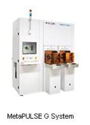
Rudolph Technologies has entered into a new market for metrology by delivering its first MetaPULSE metrology system for measuring redistribution layers (RDL) and under bump metallization (UBM) utilized in sophisticated back-end packaging technologies of the integrated circuit (IC) production process.

Rudolph Technologies’ MetaPULSE system is a well-established product used for measuring metal interconnects and opaque materials accurately and rapidly in front-end wafer processing applications. The company had shipped its first MetaPULSE system for back-end applications in the fourth quarter of 2011 and the tool was then deployed at the customer’s facility.
UBM and RDL have been utilized by IC manufacturers in sophisticated packaging processes to direct myriad I/O signal between the external world and the circuit. Measurement of pattern-dependent deposition effects must be done on patterned product wafers instead of unpatterened monitor wafers utilized in earlier process generations. The MetaPULSE system is capable of offering non-destructive measurements with speed, precision and tiny spot size necessary for measurements on patterned wafers. Moreover, the tool is capable of measuring every layer inside the finished multilayer stack or individual layers when they are deposited.
The Director of Product Management for Metrology at Rudolph Technologies, Tim Kryman commented that this development is the result of an assessment program, which the company started well before a year ago. The company partnered with a leading IC manufacturer that envisaged the necessity for on-product metrology due to the introduction of pattern-dependent deposition effects caused by rising pattern densities and reducing feature sizes in its plating process. The company is now working with several foundry, memory, and logic customers for use in more crucial back-end applications, Kryman concluded.