A team of researchers at IBM Research – Zurich, the University of Wisconsin-Madison and the University of Pennsylvania has developed a nano-sized silicon carbide tip that has a wear resistance of 10,000 folds higher than that of the earlier designs, a major breakthrough in nanomanufacturing for applications such as biosensors for environment and healthcare monitoring.

The novel nano-sized silicon carbide tip wears away at a rate below one atom/mm of sliding over a silicon dioxide substrate, a very-low value when compared to the wear rate of traditional silicon tips. It has a 100-fold greater hardness when compared to the groundbreaking silicon oxide-doped diamond-like carbon tips fabricated by the same research group last year.
The researchers have developed a novel process for fabricating the nano-sized silicon carbide tip. In the process, exposure of nanoscale silicon tip surfaces to carbon ions took place followed by annealing process to form a strong silicon carbide layer, while maintaining the original silicon tip’s nanoscale sharpness. This novel process also ensures a strong adhesion between the underlying material and the hardened surface of the tip, resembling the hardening process of steel.
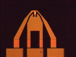
The carbide tip containing mainly silicon and carbon is then honed to a nano-sized tip and attached to a silicon microcantilever end for atomic force microscopy applications. Besides maintaining the sharpness and wear resistance, the novel process also produces the nano-sized tip with an endurance that allows it to slide over a hard substrate like silicon dioxide. It is highly important because silicon is used in all types of IC devices and exists in its oxide form in the atmosphere, making the system ideal for emerging applications in nanomanufacturing and nanolithography.
The nano-sized silicon carbide tip’s superior sliding quality against silicon oxide makes it suitable for probe-based technologies. The researchers’ next step is to test the novel tip for applications, starting with nanomanufacturing.