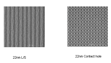
CEA-Leti has reported noteworthy advancements of the massively parallel direct write technology designed by MAPPER Lithography.

The significant accomplishment that has been achieved in resolution is 22 nm dense contact holes and 22 nm dense lines and spaces in positive chemically amplified resist. Moreover, this demonstrated resolution fulfills the industry needs for the next-generation 10 nm and 14 nm logic technology nodes.
The reported advancements are the results of the IMAGINE program’s 5th Operational Review organized by CEA-Leti from January 24 to 26, 2012. In addition, CEA-Leti and MAPPER Lithography have announced the three-year extension of the IMAGINE program with the future installation of MAPPER’s first pre-production Matrix systems at CEA-Leti, thus allowing global players to evaluate maskless lithography technology in actual production conditions.
The IMAGINE program is originally a three-year research/industry multi-partner program headed by CEA-Leti and also includes major semiconductor producers, STMicroelectronics and TSMC. Over 50 representatives from 13 different participating companies of the IMAGINE project had participated in the Operational Review event.
In this event, CEA-Leti has presented the latest advancements that include a stitching demonstration achieved on MAPPER Lithography’s pre-alpha platform deployed in CEA-Leti’s cleanroom since mid of 2009.
The Chief Executive Officer at MAPPER Lithography, Bert Jan Kampherbeek stated that the company will wrap up its Matrix pre-production platform in 2012, with an initial throughput capability of one wafer/h, which is scalable up to 10 wafers/h.
According to Laurent Malier, Chief Executive Officer at CEA-Leti, the results of IMAGINE program represents CEA-Leti’s commitment to encourage this potential lithography solution.