Researchers at Massachusetts Institute of Technology (MIT) have made an innovative approach to create three dimensional microchips using the existing production processes.
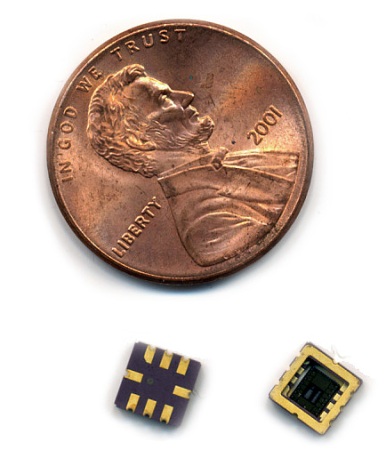
 A new approach helps researchers make tiny three-dimensional structures. Pictured are two packaged microchips, each with tiny bridges fabricated on their surfaces.
The MIT researchers have developed a MEMS device that allows 3-D sensing on only one chip.
Commonly, two dimensional MEMS devices are manufactured for detecting acceleration processes. Generally, researchers thought that devising three dimensional MEMS involves costly and complicated processes to merge many devices with accurate orientation.
Many researchers attempted to develop three dimensional devices using polymers. These devices were fabricated using lithography and were used in cogs, micro-turbines and small gears.
A postdoctoral fellow from Department of Aeronautics and Astronautics, Fabio Fachin said that silicon, due to its resistance to temperature and durability, can be replaced to polymers. However, he added that the fabrication process is difficult in silicon.
For fabrication, the engineers used a deep reactive ion etching method. Using this method, two dimensional structures are carved into a wafer. Even this method produces only a partial 3-D configuration, because the structures rise over the surface of the chip. Further, the MEMS engineers fabricated the cantilevers or small two-dimensional bridges over the surface of the chip. Finally, with high accuracy, a little force was employed to fix the bridge into the structure.
The team used a residual stress, to overcome the difficulty in the final step of the process. In every bridge structure lays a residual stress even after the disappearance of the applied force. Fachin’s group of researchers followed a previous study, which elaborates about microbeam configurations and formed equational relationship between the residual stress and the flexibility and geometry of a thin material. These calculations were used to modify the bridges to produce the required shape. This analytical tool was used to configure three dimensional devices.
An Associate Professor in aeronautics and astronautics of MIT, Brian Wardle and
Stefan Nikles from MEMSIC co worked with Fachin to develop three dimensional devices.
The Journal of Microelectromechanical Systems has agreed to publish this study