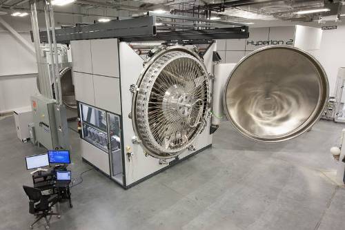
Twin Creeks Technologies, a provider of thin crystalline wafer manufacturing equipment for the semiconductor and solar industries, has launched the Hyperion production system for manufacture of ultra-thin wafers.
 Twin Creeks Technologies Hyperion 3 manufacturing tool
Hyperion 3 is the third-generation system in its line and is the first system being offered for commercial purposes. It drastically reduces the amount of substrate materials required by up to 90%. Hyperion utilizes Proton Induced Exfoliation (PIE) technology to generate monocrystalline wafers, which have a thickness that is lesser than 1/10th the thickness of standard wafers. This aspect can lead to significant savings during the manufacture of solar cells. The PIE technology prevents wastage of silicon material.
The capabilities for wafer slicing influence the thickness of wafers. The CEO of Twin Creeks, Dr. Siva Sivaram stated that only the substrates’ top most layer plays an important role in transmitting or generating signals. The other layers are wasted, he added.
The PIE technology in the Hyperion system uses atoms like a scalpel. The system implants a layer of hydrogen ions, which are high-energy protons, to a depth of 20 ì. This layer expands when heated and cleaves the top most surface of the donor wafer leading to the formation of an ultra-thin wafer. This wafer is similar to the original and can be made into semiconductors and solar modules.
The thin crystalline wafers are lighter than standard cells and solar cells manufactured with these wafers can be bent. This quality enables the feasibility of using flexible encapsulants and packaging. The lighter packaging and cost effectiveness will help Hyperion users to expand to consumer electronics and building-integrated photovoltaics (BIPV).
Twin Creeks has developed heterojunction solar cells, which are a combination of amorphous and crystalline silicon. The company has also developed intellectual property regarding ultra-thin wafers.