A team of researchers from the National Institute of Standards and Technology (NIST), the Royal Institute of Technology, and the University of Maryland Nanocenter has developed a new technique to identify flaws in nano-scale magnetic structures, even when they are buried beneath the surface of a multilayer electronic device.
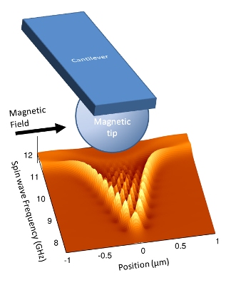
 Trapped beneath the magnetic tip of a microscale cantilever, spin waves can be used to non-destructively measure the properties of magnetic materials and search for nanoscale defects, especially in multilayer magnetic systems like a typical hard drive, where defects could be buried beneath the surface. (Credit: McMichael/NIST)
The method tested at the NIST Center for Nanoscale Technology (CNST) is based on the research conducted by scientists at the Ohio State University. The concept is to confine and image a magnetic field’s oscillating perturbations called as spin waves in a thin film. These confined spin waves can be used as a tool to measure the magnetic material properties without causing damage and detect the nanoscale defects, which may or have produced memory failures.
Robert McMichael, a researcher at NIST, explained that when a material's magnetization is hit by microwaves, it creates a ripple with spin waves because the microwave energy impels the spins, which in turn impel other spins. The microwaves are tuned to a frequency just beyond the range wherein the propagation of the spin waves occurs, excluding the area right beneath the magnetic probe tip.
Flaws in the material disturb the confined spin waves to cause an effect, which enables the characterization of the defects on 100 nm length scales. Earlier study had demonstrated this effect in magnetic spins, which were vertically oriented to the surface of the magnetic film, thus limiting the resolution because the individual spins were strongly connected with other spins.
In this work, the magnetic spins are not strongly coupled and are arranged in a plane with each other. This pattern not only resembles the structure of most of the magnetic devices but also enables closer focusing and higher resolution.