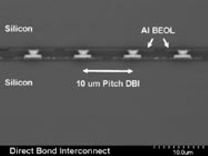
Ziptronix, whose trademark Direct Bond Interconnect (DBI) technology facilitates reduction in footprint and the size of devices with 3D architecture, has announced its collaboration with a new customer to extend the DBI technology to 3D memory applications.
 DBI technology
Memory stacking, which essentially entails stacking memory chips on top of one another, provides significant benefits by way of space conservation on the circuit board and improved electrical performance due to faster propagation of signals owing to shorter interconnections. The conventional technology in practice is however plagued by problems such as high processing costs, need for reliable interconnection and facility to handle thinned dies.
Ziptronix DBI eliminates the limitations of die stacking technology by adopting oxide bonding at the wafer level itself at low temperature. Since these are low-stress albeit strong bonds, the wafers can be processed and thinned easily even after bonding. Ziptronix DBI has already established its comparative benefits vis-à-vis copper thermo-compression bonding in the Backside Image Sensing (BSI) market. DBI maximizes accuracy of component alignment and also the density of the interconnecting paths between elements. It allows damascene processing of interconnections, maximizes vertical stacking density by virtue of its uniform and high bonding capability and facilitates the performance of a host of post-bonding tests.
Dan Donabedian, CEO of Ziptronix, stated that the collaboration with their new customer was an acknowledgement of the technology’s success in the image sensor sphere and that the company would be shortly making announcements pertaining to licensing agreements with silicon-based manufactures outside the image sensor realm.