A research team from the Argonne National Laboratory of the US Department of Energy has devised a novel technique that is capable of drastically enhancing the efficiency and lowering the cost of fabricating various types of semiconducting materials.
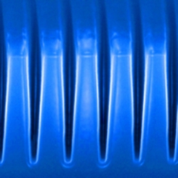
 This image shows channels etched using sequential infiltration synthesis, which scientists at Argonne have used to create features that have high aspect ratios – that is, they are far deeper than wide. These crevasses will permit the creation of a new generation of semiconducting materials
The innovative technique fulfills certain prerequisites of the international semiconductor ‘roadmap’ for 2022. At present, photolithography is used to make semiconductor patterns by selectively removing parts of a thin film. Etching of a pattern, also known as resist, into the semiconductor is done by exposing to an ionized gas. However, the resist is also etched away by this gas, thus decreasing the reusability of this film. Highly durable resists are termed as hard masks.
Seth Darling, a nanoscientist at Argonne National Laboratory, informed that domain collapse is a barrier to fabricate smaller semiconductor components. Researchers are still not able to find a solution to eliminate this collapse.
Darling and colleagues devised a method called sequential infiltration synthesis (SIS) in 2010. The technique grows tough inorganic materials within a soft polymer film using gases. The DOE Office of Science supported the research via the Argonne-Northwestern Solar Energy Research Center and Argonne’s Center for Nanoscale Materials.
SIS avoids the use of hard masks in photolithography, said Darling. This is one of the major advantages of SIS as hard masks are complex, high-cost, decrease pattern quality and increase process steps. Major semiconductor companies have already recognized SIS as a technology capable of addressing various complex challenges.
Darling and colleagues recently demonstrated SIS’ capability of eliminating pattern collapse and allowing the production of materials with higher aspect-ratio patterns. Darling stated that one of the key benefits of this demonstration is the possibility of utilizing SIS for photolithography, a critical industrial process.