Researchers believe that indium gallium nitride, part of III-nitrides family, is an ideal material for photovoltaic applications because by altering indium concentration the material’s response can be tuned to collect solar energy from different wavelengths.
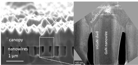
 Cross-sectional images of the indium gallium nitride nanowire solar cell. (Image courtesy of Sandia National Laboratories)
However, structural strain is a major issue of indium gallium nitride, which is usually grown over thin gallium nitride films. The difference in crystal lattice spacings between indium gallium nitride atomic layers and gallium nitride atomic layers results in structural strain, which limits indium concentration and layer thickness.
To overcome this issue, George Wang and Jonathan Wierer Jr., researchers at Sandia National Laboratories, have discovered a way by growing indium mixture on a phalanx of nanowires instead on a flat surface. The nanowires’ small surface area eases strain by enabling partial relaxation of the indium shell layer along each wire. This enables the researchers to develop a nanowire solar cell containing approximately 33% of indium, a much higher value when compared to other III-nitride solar cells.
Moreover, this work also achieved a reduction in absorption base energy from 2.4 eV to 2.1 eV, which is the lowest reported value to date for an III-nitride solar cell. In addition, it enabled the availability of a broad range of wavelengths for power conversion. However, power conversion efficiency is mere 0.3%, which is comparatively much lower than 15% conversion efficiency of a typical commercial cell. Nevertheless, fine tuning the imperfections in nanowire-array templates must result in higher conversion efficiencies and lower energies.
The researchers used various novel methods to fabricate the III-nitride nanowire array solar cell. To form the nanowire array, they used a top-down fabrication process wherein a colloidal silica mask is used to mask a gallium nitride (GaN) layer, which is then dried and wet etched. This resulted in an array comprising evenly heighted nanowires with vertical sidewalls. They then used a metal organic chemical vapor deposition method to form shell layers comprising the higher indium content indium gallium nitride (InGaN) on the GaN nanowire template. Finally, In0.02Ga0.98N was formed that resulted in coalescing of nanowires. The technology is manufacturable as it enables simple planar processing.
Besides enabling higher indium concentration in the InGaN layers, the nano-architecture increased absorption through light scattering in the InGaN canopy layer and air voids that direct light inside the nanowire array.