MOSIS, a provider of low-cost prototyping and small volume production services for custom ICs, teams up with imec, Tyndall and ePIXfab -- the European Silicon Photonics support center providing low-cost prototyping services for photonic ICs.
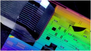
 Packaged passive silicon photonics chip. Imec, silicon photonic chip; Tyndall, fiber array packaging.
The partnership gives MOSIS' customers access to imec's state-of-the-art fully integrated silicon photonics processes and Tyndall's advanced silicon photonics packaging technology.
Imec's silicon photonics platform enables cost-effective R&D of silicon photonic ICs for high-performance optical transceivers (25Gb/s and beyond) for telecom, datacom, and optical sensing for life science applications. The offered integrated components include low-loss waveguides, efficient grating couplers, high-speed silicon electro-optic modulators and high-speed germanium waveguide photo-detectors. A comprehensive design kit to access imec technologies will be provided. Moreover, the Tyndall National Institute, being a partner of ePIXfab, offers the ability to provide packaged silicon photonics devices. This includes the design and fabrication of custom photonic packages, fiber coupling (single and arrays) and electrical interconnects. Design rules to support these packaging capabilities will also be provided.
"Imec's Silicon Photonics platform provides robust performance, and solutions to integrated photonics products. Companies can benefit from imec silicon photonics capability through established standard cells, or explore the functionality of their own designs in MultiProject Wafer runs," stated Philippe Absil, program director at imec. "With this collaboration, MOSIS will offer its first access to a mature Silicon Photonics infrastructure, with the option for follow-on production," added Wes Hansford, MOSIS Director.
The first ePIXfab-Europractice run for passive silicon photonics ICs is open for registration from June 2013 with design deadline September 9th 2013. MOSIS' customers can register for this run and obtain the design kit via MOSIS in June 2013.
Imec's Si Photonics 200mm wafer platform offers extensive design flexibility and includes:
- Tight within-wafer silicon thickness variation 3sigma < 2.5nm
- 3-level patterning of 220nm top Si layer (193nm optical lithography)
- poly-Si overlay and patterning (193nm optical lithography)
- 3-level n-type implants and 3-level p-type implants in Si
- Ge epitaxial growth on Si and p-type and n-type implants in Ge
- Local NiSi contacts, Tungsten vias and Cu metal interconnects
- Al bond pads
- Validated cell library with fiber couplers, polarization rotators, highly efficient carrier depletion modulators and ultra-compact Ge waveguide photo-detectors with low dark current.
- Design kit support for IPKISS framework, PhoeniX Software and Mentor Graphics software
Tyndall's Si Photonics Packaging Technology enables
- Passive device packaging, single and multi-fiber arrays to grating couplers
- Active device packaging, modulators and detectors with electrical ports and fiber arrays
- Custom packaging requirements (mechanical, thermal stability etc.)