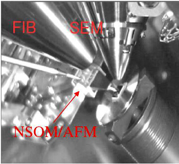
Nanonics is proud to announce that our triple beam integrated AFM/SEM/FIB system, the Nanonics 3TB4000, was judged one of the ten best microscopy innovations in 2013 and is the recipient of the prestigious 2013 Microscopy Today Innovation Award.
 The award‐winning Nanonics3TB4000, an integrated AFM/SEM/FIB system
The 3TB4000 provides the ultimate 3D nanoscale characterization capability through a revolutionary innovation of open architecture that provides open access to the SEM/FIB beams without any obstruction or interference to the injectors, detectors, or beam lines.
With the 3TB4000, the SEM, FIB, and AFM can now be used to provide complimentary information in order to provide a complete characterization of material by taking advantage of the functional and high resolution 3D capabilities of AFM, the large field of view and rapid scanning of the SEM, and the fabrication/material removal capability of the FIB.
Applications demonstrating this powerful new capability have been shown in diverse areas including sidewall imaging in semiconductors, locating and measuring optical properties of individual metal oxide nanowires or mechanical properties of surface features, and assessing AFM probes in situ while imaging. For more information, please contact Nanonics at [email protected] or visit our website at www.nanonics.co.il.
About Nanonics Imaging Ltd
Nanonics Imaging is the premier innovator of AFM and NSOM systems in the SPM market. Since its inception in 1997 and throughout the last fifteen years Nanonics have introduced new concepts in system functionality to the SPM market, which in turn have supported the pursuit of new areas of scientific application.
Nanonics contributions span from our revolutionary approach to NSOM imaging with cantilevered NSOM probes, to our introduction of dual tip/sample scanning AFM systems; and from our introduction of the first ever NSOM/AFM cryogenic systems to the first ever, Raman/AFM, Multiprobe AFM and SEM/AFM systems.