A team of researchers from the University of California, Riverside's Bourns College of Engineering have solved a problem that previously presented a serious hurdle for the use of graphene in electronic devices.
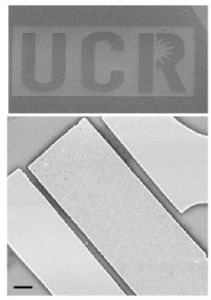
 Scanning electron microscopy image of graphene device used in the study. The scale bar is one micrometer. The UCR logo next to it is implemented with etched graphene.
Scanning electron microscopy image of graphene device used in the study. The scale bar is one micrometer. The UCR logo next to it is implemented with etched graphene.
Graphene is a single-atom thick carbon crystal with unique properties beneficial for electronics including extremely high electron mobility and phonon thermal conductivity. However, graphene does not have an energy band gap, which is a specific property of semiconductor materials that separate electrons from holes and allows a transistor implemented with a given material to be completely switched off.
A transistor implemented with graphene will be very fast but will suffer from leakage currents and power dissipation while in the off state because of the absence of the energy band gap. Efforts to induce a band-gap in graphene via quantum confinement or surface functionalization have not resulted in a breakthrough. That left scientists wondering whether graphene applications in electronic circuits for information processing were feasible.
The UC Riverside team – Alexander Balandin and Roger Lake, both electrical engineering professors, Alexander Khitun, an adjunct professor of electrical engineering, and Guanxiong Liu and Sonia Ahsan, both of whom earned their Ph.Ds from UC Riverside while working on this research – has eliminated that doubt.
"Most researchers have tried to change graphene to make it more like conventional semiconductors for applications in logic circuits," Balandin said. "This usually results in degradation of graphene properties. For example, attempts to induce an energy band gap commonly result in decreasing electron mobility while still not leading to sufficiently large band gap."
"We decided to take alternative approach," Balandin said. "Instead of trying to change graphene, we changed the way the information is processed in the circuits."
The UCR team demonstrated that the negative differential resistance experimentally observed in graphene field-effect transistors allows for construction of viable non-Boolean computational architectures with the gap-less graphene. The negative differential resistance – observed under certain biasing schemes – is an intrinsic property of graphene resulting from its symmetric band structure. The advanced version of the paper with UCR findings can be accessed at http://arxiv.org/abs/1308.2931.
Modern digital logic, which is used in computers and cell phones, is based on Boolean algebra implemented in semiconductor switch-based circuits. It uses zeroes and ones for encoding and processing the information. However, the Boolean logic is not the only way to process information. The UC Riverside team proposed to use specific current-voltage characteristics of graphene for constructing the non-Boolean logic architecture, which utilizes the principles of the non-linear networks.
The graphene transistors for this study were built and tested by Liu at Balandin's Nano-Device Laboratory at UC Riverside. The physical processes leading to unusual electrical characteristics were simulated using atomistic models by Ahsan, who was working under Lake. Khitun provided expertise on non-Boolean logic architectures.
The atomistic modeling conducted in Lake's group shows that the negative differential resistance appears not only in microscopic-size graphene devices but also at the nanometer-scale, which would allow for fabrication of extremely small and low power circuits.
The proposed approach for graphene circuits presents a conceptual change in graphene research and indicates an alternative route for graphene's applications in information processing according to the UC Riverside team.