Jun 17 2014
Physicists at the University of Rochester have created a silicon nanocavity that allows light to be trapped longer than in other similarly-sized optical cavities. An innovative design approach, which mimics evolutionary biology, allowed them to achieve a 10-fold improvement on the performance of previous nano cavities.
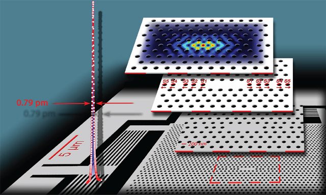
 Light-trapping nanostructure created by the researchers: The top layer shows a simulation of the nanostructure confining the light in the tiny red regions. The second layer is the design generated by an approach that mimics evolutionary biology. The bottom two layers show electron micrographs of the realized nanostructure in silicon. The sharp peak on the left is the trace of the long trapping of light. Credit: Fabio Badolato
In a paper published in Applied Physics Letters today and featured on the cover, the scientists demonstrate they have confined light in a nanocavity – a nanostructured region of a silicon wafer – for nanoseconds. Typically light would travel several meters in that time, but instead the nanostructure confined light in a region no bigger than one one hundredth the width of a human hair – roughly one-half millionth of a meter.
“Light holds the key to some of nature’s deepest secrets, but it is very challenging to confine it in small spaces,” says Antonio Badolato, professor of physics at the University of Rochester and corresponding author of the Applied Physics Letters paper. “Light has no rest mass or charge that allow forces to act on it and trap it; it has to be done by carefully designing tiny mirrors that reflect light millions of times.”
Nanocavities are key components of nanophotonics circuits and Badolato explains that this new approach will help implement a new-generation of highly integrated nanophotonics structures.
Researchers are interested in confining light because it allows for easier manipulation and coupling to other devices. Trapping light also allows researchers to study it at its fundamental level, that is, at the state when light behaves as a particle (an area that led to the 2012 Nobel Prize in Physics).
Until now, researchers have been using educated-guess procedures to design the light-trapping nanostructures. However in this case, the team of researchers – which included lead author and Badolato’s Ph.D. student, Yiming Lai, and groups from the Ecole Polytechnique Federale de Lausanne, Switzerland, and the Universita di Pavia, Italy– perfected a numerical technique that lead to the design improvement. Their computational approach allowed them to search for the optimal combination of parameters among thousand of realizations using a “genetic” (or “evolutionary”) algorithm tool.
The principle behind the genetic approach is to regard each new nanocavity as an individual in a population. The individuals mutate and “breed,” meaning that two single structures combine to create a new one that is a cross between the two “parents.” As new generations succeeded one another, the algorithm selected the fittest ones in each generation, in this case, the ones that exhibited the longest trapping time (i.e. highest quality factor).
Integrated nanophotonics is a new and rapidly growing field of research laying at the intersection of photonics, nanotechnology, and materials science. In the near future, nanophotonics circuits will enable disruptive technologies ranging from telecommunications to biosensing, and because they can process pulses of light extremely fast and with very low energy consumption, they hold the potential to replace conventional information-handling systems.
The results shown by Badolato and his colleagues demonstrate one of the highest quality factors ever measured in nanocavities while maintaining a very small footprint. By keeping the nanocavities so small while trapping light so efficiently it becomes possible to create devices with ultra-dense integration – a desired characteristic in the fabrication of optical nano circuits.
The extreme sensitivity of these nanocavities to tiny changes in the environment, for example a virus attaching near the area where light is trapped, makes these devices particularly appealing for biosensing. By using these highly sensible nanocavities, such a biosensing device could detect minute quantities of these biomaterials by analyzing a single drop of blood. Badolato’s group is now starting a collaboration with researchers at the University of Rochester’s Medical Center to exploit this interesting property with the new nanocavities.