Eulitha AG's revolutionary PHABLE photolithograhy technology for low-cost printing of photonic patterns is continuing to attract interest from the industry and research fields. The latest example is a China based manufacturer of specialty optical components.

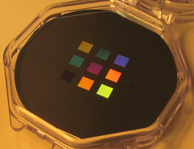
Diffraction gratings printed on PhableR 100
After evaluating the alternatives including nanoimprint lithography the company decided to go with Eulitha's unique PhableR 100 system due to its significant process and cost advantages. With the PhableR 100 system, many different types of gratings and photonic crystal type patterns can be realized with a robust photolithographic exposure. The system was delivered and qualified in the final days of 2014. Eulitha will continue to support the production of the customer with specialty photomasks and process support.
The PhableR 100 system is capable of exposing periodic patterns down to feature sizes below 150nm which rivals high-end i-line steppers. The focus-free image formed by the system enables uniform printing on non-flat samples often found in photonic and optoelectronic sectors.
Sales Director of Eulitha, Rene Wilde said "We are very happy with the market reaction to the unique value offered by our breakthrough technology in manufacturing and research environments. Production of patterned sapphire substrates (PSS) and light extraction structures on LEDs remains to be our main focus but this adoption by an optical manufacturer demonstrates the wide ranging application field for our novel technology."

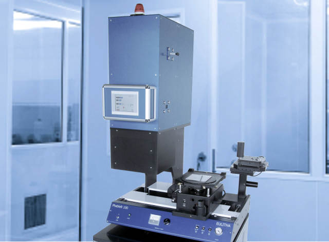
PhableR 100 photolithography system
About Eulitha AG
Eulitha AG is a spin-off company of the Paul Scherrer Institute, Switzerland. It specializes in the development of lithographic technologies for applications in optoelectronics and photonics. It produces and markets nano-patterned samples and templates using its own PHABLE tools and state-of-the-art e-beam lithography systems. PHABLE is a registered trade mark and the brand name of Eulutha's proprietary photolithography platform, which includes exposure tools and wafer patterning services.