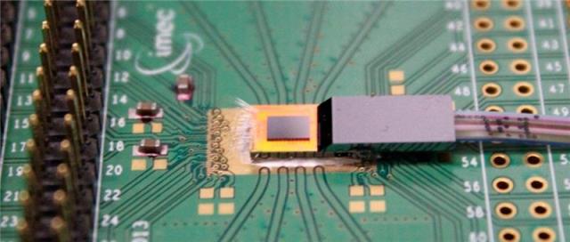
Today, at the 2015 International Solid State Circuits Conference (ISSCC), nanoelectronics research center imec, in collaboration with Tyndall National Institute, the University of Leuven (KULeuven) and the Ghent University, demonstrated a 4x20Gb/s wavelength division multiplexing (WDM) hybrid CMOS silicon photonics transceiver, paving the way to cost-effective, high-density single-mode optical fiber links.

Hybrid CMOS silicon photonics transceivers, transmitting and receiving data over single-mode optical fiber, are expected to play a key role in next-generation datacenter connectivity. By leveraging existing CMOS manufacturing and 3-D assembly infrastructure, the hybrid CMOS silicon photonics platform enables high integration density and reduced power consumption, as well as high yield and low manufacturing cost. Combined with wavelength division multiplexing capability, highly scalable single-mode optical transceivers can be constructed, satisfying the growing need for interconnect bandwidth in next-generation cloud infrastructure.
Imec’s CMOS silicon photonics transceiver comprises a silicon photonics (SiPh) chip, flip-chip integrated with a low-power 40nm CMOS chip. The SiPh chip, fabricated on imec’s 25Gb/s Silicon Photonics Platform (iSiPP25G), comprises an array of four compact 25Gb/s ring modulators, coupled to a common bus waveguide to allow WDM transmission. On the receive side, a ring-based, low-loss (2dB) demultiplexing filter with 300GHz channel spacing is implemented and further connected to an array of four 25Gb/s Ge waveguide photodetectors. Both the ring modulators and the ring WDM filters include highly efficient integrated heating elements to tune their resonant wavelengths to the desired WDM channels. The CMOS chip includes four differential 20Gb/s ring modulator drivers and four 20Gb/s trans-impedance amplifiers. A 12 channel single-mode fiber array is packaged onto the grating coupler array on the chip, using a planar approach developed at Tyndall National Institute.
Error-free operation was demonstrated in a 20Gb/s loop-back experiment for all four WDM channels as well as with two channels running together. The dynamic power consumption of the transceiver, including the CMOS driver and receiver, was less than 2pJ/bit. Thermal tuning of the WDM channel wavelengths consumed only 7mW/nm per channel. The transceiver can be further scaled to higher bandwidth capacity by adopting more advanced CMOS technology and by adding more WDM channels, enabling optical modules for 100GbE, 400GbE and beyond for future datacenter interconnects.
This work was supported by imec’s optical I/O core partner program. Imec’s iSiPP25G technology can be accessed through Europractice, while Si Photonics packaging services are available through Tyndall National Institute (Ireland).