Feb 28 2015
A European research project has made an important step towards the further miniaturisation of nanoelectronics, using a highly-promising new material called silicene. Its goal: to make devices of the future vastly more powerful and energy efficient.

Silicene, a new semiconducting material combining properties of silicon and graphene, is one of the most promising candidates for manufacturing even tinier electronic circuitry for future smart devices.
‘Electronics are currently embedded in many layers of silicon atoms. If they can be manufactured in a single layer, they can be shrunk down to much smaller sizes and we can cut down on power leakage, at the same time making devices more powerful and energy efficient,’ explained Dr Athanasios Dimoulas, coordinator of the EU’s 2D-NANOLATTICES project.
Graphene is an interesting substance in that it occurs in a single layer of atoms, but does not have the ‘energy gap’ needed to be a semiconductor material. Silicene, a 2D form of silicon, brings its semiconductor properties into the world of 2D materials. The problem with silicene, however, is it is modified in contact with other substances such as metals.
Electronics that are 100 times smaller
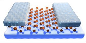
Condensing electronics into a single layer of silicene and retaining electronic performance has proved a difficult task for researchers – until now that is. The 2D-NANOLATTICES project has achieved a significant innovation worldwide by making a Field Effect Transistor (FET) out of the material to operate at room temperature.
FETs are a key switching component in electronic circuitry. Embedding it into just one layer of silicon atoms (in silicene structure), then transferring the layer, grown on a silver substrate, to one made of a more neutral substance, silicon dioxide, is a considerable success. ‘Tests showed that performance of silicene is very, very good on the non-metal substrate,’ enthused Dr Dimoulas, of Demokritos, Greece’s National Center for Scientific Research.
‘The fact that we have this one transistor made of just one single layer of material like silicon has not been done before and this is really something that can be described as a breakthrough. On the basis of this achievement, it could be possible to make transistors up to 100 times smaller in the vertical direction,’ Dr Dimoulas added.
Seeing the potential
Now that the transistor has been shrunk vertically into just one 2D layer of atoms, the dimensions can be shrunk laterally, too, meaning the same area on a chip could accommodate up to 25 times more electronics, Dr Dimoulas calculated.
Additionally, the use of a single, narrow channel to conduct electrical current reduces power leakages, a problem that has been worrying the semiconductor industry for some time: how to go even smaller without devices overheating in the form of power leakage.
This is good news for chip manufacturers, as the race to produce the next wave of communications technologies hots up with the advent of 5G mobile networks.
2D NANOLATTICES, which received EUR 1.63 million of funding from FP7 (through the Future and Emerging Technologies scheme), took place from 1 June 2011 till 31 August 2014 and consisted of six partners, in four EU countries.