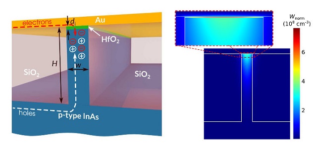
 Schematic of the electrically pumped active hybrid plasmonic waveguide and energy density distribution of the surface plasmon field.
The novel method, developed at the Laboratory of Nanooptics and Plasmonics at the MIPT Center of Nanoscale Optoelectronics, could help reduce the size of optoelectronic and optical elements, and boost the performance of computers. It would also enable elimination of energy losses of surface plasmons used in optical devices.
Surface plasmon polaritons have previously been proposed to be used as information carriers for optical communication, but the problem is that the signal is rapidly attenuated propagating along plasmonic waveguides. Now, we have come very close to the complete solution of this problem. Our approach clears the way for the development of a new generation of high performance optoelectronic chips.
Dmitry Fedyanin, the head of the research
Electrons are used as information carriers in modern electronics. However, they are not able to meet the current requirements of modern microprocessors. The commonly used electrical copper wires and the channels on chips do not have the capability to transfer information at speeds that are required for present day microprocessors. This affects the performance growth of microprocessors. In order to maintain Moore's law, advanced new technologies have to be implemented.
The use of optical pulses in place of electrical pulses could help address this problem. Light waves have a high frequency, in terms of hundreds of terahertz, which would enable them to process and transfer more data, thereby enhancing their performance. Fiber optic technologies are being commonly utilized in optical communication networks.
However, the problem of diffraction limit has curtailed the utilization of light in logical elements and microprocessors. This is because the size of optical elements, including the size of waveguides, cannot be smaller than the wavelength of light. In optical communications, micrometers for near-infrared radiation are used; however, they are not capable of addressing the needs of modern electronics. In standard contemporary processors, their logical elements are in the nanoscale, and hence, only when light is “compressed” to this scale, optical electronics can become viable.
Transitioning to surface plasmon polaritons from photons could help address the problem of diffraction limit. Surface plasmon polaritons are collective excitations that take place when interaction occurs between electron oscillations and photons at a metal-insulator boundary. Due to their properties, these polaritons are also called as quasi-particles, as they are similar to photons, electrons and other such standard particles. Surface polaritons have the ability to “hold on” to the boundary that exists between two media, which is not possible by three-dimensional light waves. This may allow switching from traditional three-dimensional optics to two-dimensional optics.
Roughly speaking, a photon occupies a certain volume in space, which is of the order of the light wavelength. We can “compress” it, transforming into a surface plasmon polariton. Using this approach, we can improve the integration density and reduce the size of optical elements. Unfortunately, this brilliant solution has its flip side. For the surface plasmon polariton to exist, a metal, or more specifically, an electron gas in the metal, is needed. This leads to excessively high Joule losses similar to those one has when the current is passed through metal wires or resistors.
Dr. Fedyanin.
Fedyanin states that due to absorption in the metal, surface plasmon energy gets reduced a billion times at distances of approximately one millimeter. Hence, practically implementing surface plasmons serves no purpose.
"Our idea is to compensate the surface plasmon propagation losses by pumping extra energy to surface plasmon polaritons. It should be also noted that, if we want to integrate plasmonic waveguides on a chip, we can use only electrical pumping," explains the researcher.
Along with colleagues Dmitry Svintsov and Aleksey Arsenin from the Laboratory of Nanooptics and Plasmonics, Dr. Fedyanin has developed a novel method for electric pumping of plasmonic waveguides. This method is based on the metal-insulator-semiconductor (MIS) structure. The researchers performed simulations that revealed that the relatively weak pump current’s passage through the nanoscale plasmonic waveguides could completely compensate the losses due to surface plasmon propagation. Hence, this would mean that a signal could be transmitted without any losses over long distances. Furthermore, these active plasmonic waveguides have an integration density that is very much higher when compared to that of photonic waveguides.
Working in optoelectronics, we always need to find a compromise between optical and electrical properties, whereas in plasmonics it is almost impossible, since the choice of metals is limited to three or four materials. The main advantage of the proposed pumping scheme is that it doesn't dependent on the properties of the metal-semiconductor contact. For each semiconductor, we can find an appropriate insulator, which allows to achieve the same efficiency level as in double-heterostructure lasers. At the same time, we are able to maintain the typical plasmonic structure size at a level of 100 nanometers.
Fedyanin.
The team states that the main difficulty has been addressed, and the results of the study have to be verified experimentally.
The research paper has been published in Optics Express.
The Russian Science Foundation and the program for improving the competitiveness of MIPT have supported this study.
References