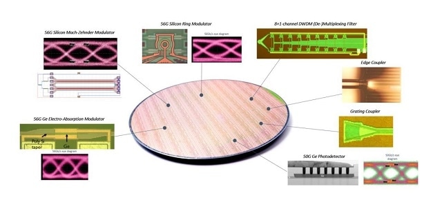
World-leading nanoelectronics research center imec presents at OFC 2016, the international event for both the science and business of optical communications held March 20-24, performance improvements of various key building blocks of its wafer-scale integrated silicon photonics platform (iSiPP)
The new results expand imec’s iSiPP device portfolio to support 50Gb/s non-return-to-zero (NRZ) lane rates, and are an important milestone for the realization of high data rate silicon integrated optical interconnects targeting high density, high bandwidth, low power telecom and datacom transceivers, as well as for low cost large volume applications such as sensors or LiDAR.
Through process and design optimizations, imec has improved the operating speed of the silicon based traveling-wave mach-zehnder modulators and ring modulators to reach 50Gb/s NRZ lane rates. In addition, a C-band GeSi electro-absorption modulator was developed with electro-optical bandwidth beyond 50GHz, enabling NRZ modulation at 56Gb/s and beyond.
All modulator types can be driven with competitive drive voltages of 2Vpp or below, enabling compatibility with power efficient CMOS driver circuits.
The responsivity of the high-speed Ge photodetectors has been improved to 1A/W, enabling highly sensitive 50Gb/s NRZ receivers both in the C-band and the O-band. Also, edge coupling structures were developed for broadband optical coupling to high- NA and lensed fiber with less than 3dB insertion loss in the C-band. Moreover, designers can exploit the superior patterning fidelity provided by 193-nm lithography, enabling robust active and passive waveguide devices.
The 50Gb/s components are included in imec’s 200mm silicon photonics multi-project wafer (MPW) offer, and are supported by a Process Design Kit (PDK).The MPW service is available via Europractice IC service and MOSIS, a provider of low-cost prototyping and small volume production services for custom ICs. Imec’s active iSiPP50G run is now open for registration (deadline June 28th 2016) with first wafers out in January 9th 2017.
Imec also provides technology customization options with dedicated wafer fabrication services supported by a PDK.This service enables the use of full-size reticles, delivery of full wafers, and access to specialty modules enabling high efficiency integrated heaters, MOSCAP devices and flip-chip assembly amongst others.
The PDK’s have been validated with silicon data, based on a minimum of two process runs for most of the components, and describe the process and device performance statistics.They are supported in various EDA environments and include DRC, supporting first-time right designs.