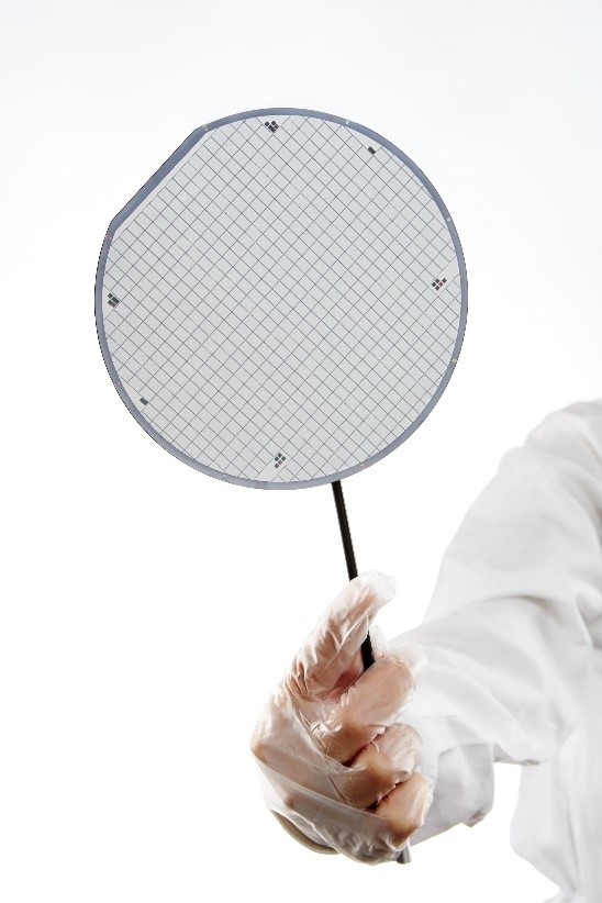
San Diego based graphene and 2D materials producer Grolltex has completed characterization and is releasing for commercial sale a configuration of large area, single layer graphene that exhibits dramatically improved ‘electron mobility’, which translates to better graphene performance. This ‘heterostructure’ contains a layer or layers of hexagonal Boron Nitride (or ‘hBN’) underneath graphene, enabling enhanced graphene capabilities.
Grolltex has begun commercial pre-sales to customers of this ‘Enhanced Performance Graphene’ product, which can significantly improve device performance for sensing, transistors, connectivity and other key aspects of nano-devices. This type of material performance improvement is often a stepping stone for new applications enabling large market growth toward faster, smaller, cheaper and more sensitive silicon-based devices.
The data back from our large European device partner showed carrier mobility performance improvements starting at 30%, and our internal work shows us that with some configuration adjustments, we can even build on this toward electron mobility improvements in exponential regimes. We believe this is going to be incredibly important to many of our customers that build things on silicon.
Jeff Draa, CEO and Co-Founder, Grolltex
The first reason for the improvement of graphene electron mobility performance, when layered on top of hBN on a wafer, is that the underlying layer of hBN, between the wafer and the graphene, planarizes the surface of the silicon wafer and allows graphene to sit on a surface (hBN) far more conducive to graphene electron flow.
Another reason has to do with the electron interference of the oxide coming out of the underlying Si/SiO2 wafer, if graphene sits directly on top of it. With the hBN layer between the graphene and the wafer, the negative effect of the oxide from the wafer on graphene electron performance is greatly reduced, allowing a much freer flow of graphene electrons. Additional advantages are lower processing temperatures and a much stronger adhesion of the graphene layer to the underlying substrate, with hBN present.
When graphene sits on hBN, it performs much closer to the theoretical ‘electron superhighway’ that graphene users expect. We have characterized and are selling this heterostructure to our pre-qualified customers in up to 8” (200mm) diameter configurations and can layer hBN and graphene in any combination. Device designers, especially advanced sensor makers, are really keyed in to electron mobility. There are many variables that affect this and he who can square those away and show dramatic improvements in mobility can help add real, unique and substantial value to device performance. Next on our characterization list is MoS2, which is an important ‘band-gap’ material that has been missing in 2D offerings.
Jeff Draa, CEO and Co-Founder, Grolltex
Grolltex, short for ‘graphene-rolling-technologies’, uses patented research and techniques initially developed at the University of California, San Diego, to produce high quality, single layer graphene, hexagonal Boron Nitride and other 2D materials and products. The company is a practitioner of, and specializes in, exclusively sustainable graphene production methods and is committed to advancing the field of graphene to improve the future of leading edge materials science and product design through the optimization of single atom thick materials.