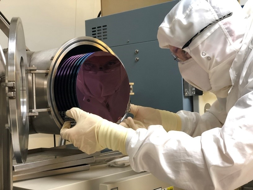
Graphene and 2D materials producer, Grolltex has completed its recent capacity expansion and released production for 30,000 eight-inch wafer equivalents per year at its CVD monolayer fabrication facility in San Diego, California. This ‘single atomic layer’ type of graphene is used in advanced electronics and other nano-devices and supports many use cases in wearables, IoT, photonics, semiconductors, biosensing and other next generation devices.

“This is the only commercial CVD monolayer graphene production facility in California and in fact it is the largest capacity plant of its kind in the U.S.”, said CEO, Jeff Draa. “Demand for our electronics grade graphene has never been better. Our production lines are capable of producing single layer graphene or single layer hexagonal Boron Nitride”.
Otherwise known as ‘white graphene’, hexagonal Boron Nitride (or ‘hBN’) is the single atom thick insulator complement to graphene, which is a conductor. The material hBN also has many other interesting characteristics, including being highly transparent, very strong, possesses anti-microbial and flame-retardant properties and is additionally a performance accelerator for graphene. The Grolltex factory expansion supports the growth, production and transfer of both of these single layer materials.
“Maybe even more exciting, we currently have four active evaluations where our customers’ advanced nano-factories are testing our graphene for use as the basis for their final devices and each factory eval is going very well”, said Draa. “The biosensing area is an early adopter for our graphene, as evidenced by customers using our material to detect DNA, find diseases in blood, monitor glucose in sweat in the form of a wearable patch and validating the safety and efficacy of new drugs in previously unthinkably short times and low costs.”
Grolltex, short for ‘graphene-rolling-technologies’, makes large area, single atom thick graphene sheets using chemical vapor deposition or ‘CVD’; essentially the process is depositing gas in a chamber, then allowing it to cool, which leaves a continuous one atom thick layer of carbon on a target substrate. This type of graphene is highly valued for its electrical characteristics, strength and flexibility and some see it as ‘next generation silicon’.
The company uses patented research and techniques initially developed at the University of California, San Diego, to produce high quality, single layer graphene, hexagonal Boron Nitride and other 2D materials and products. The company is a practitioner of, and specializes in, exclusively sustainable graphene production methods and is committed to advancing the field of graphene to improve the future of leading-edge materials science and product design through the optimization of single atom thick materials.