Mar 12 2019
With the help of a revolutionary method, researchers have discovered a novel way to apply some of the world’s most intense X-rays to reveal the way atoms move at ultrafast speeds in a single atomic sheet.
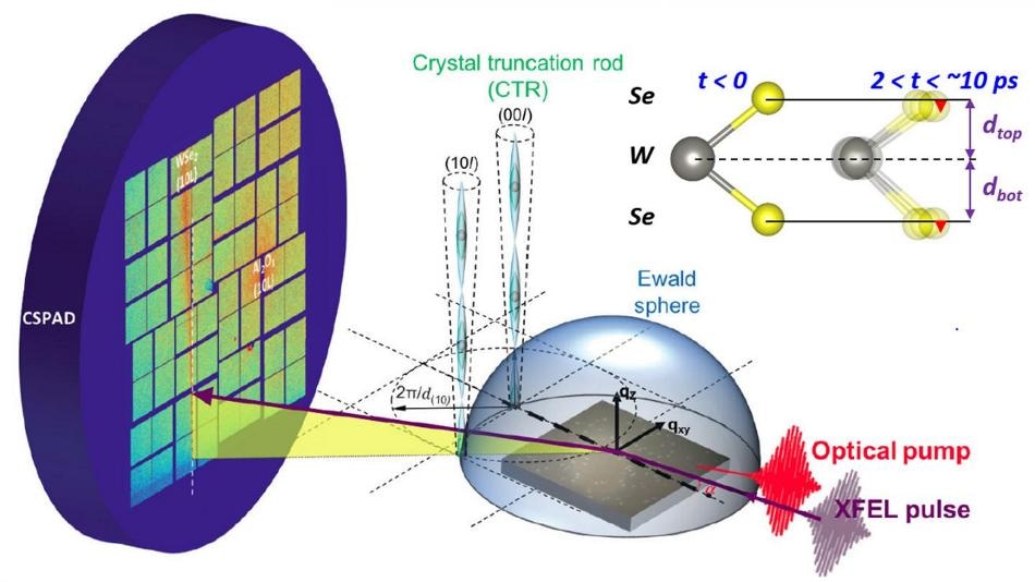
 This image shows the experimental setup for a newly developed technique: ultrafast surface X-ray scattering. This technique couples an optical pump with an X-ray free-electron laser probe to investigate molecular dynamics on the femtosecond time scale. (Image credit: Haidan Wen.)
In the study, headed by scientists at the U.S. Department of Energy’s (DOE) Argonne National Laboratory and in association with other institutions, including DOE’s SLAC National Accelerator Laboratory and the University of Washington, an innovative method known as ultrafast surface X-ray scattering was developed. The varying structure of an atomically thin two-dimensional (2D) crystal, resulting from its excitation with an optical laser pulse, was revealed by this method. In addition, the novel method is different from earlier surface X-ray scattering techniques, and in addition to giving a static picture of the atoms on the surface of a material, it also captures the movements of atoms on timescales down to trillionths of a second following laser excitation.
It is possible to perform certain time-dependent surface X-ray scattering as well as static surface X-ray scattering at a synchrotron X-ray source; however, in order to perform ultrafast surface X-ray scattering, the scientists had to employ the Linac Coherent Light Source (LCLS) X-ray free-electron laser at SLAC. Extremely bright X-rays with very short exposures of 50 femtoseconds are provided by this light source. When the researchers rapidly delivered huge quantities of photons to the sample, they successfully produced an adequately robust time-resolved scattering signal, thereby envisaging the movement of atoms in 2D materials.
Surface X-ray scattering is challenging enough on its own. Extending it to do ultrafast science in single-layer materials represents a major technological advance that can show us a great deal about how atoms behave at surfaces and at the interfaces between materials.
Hua Zhou, Study Author and X-ray Physicist, Argonne National Laboratory.
Atoms in 2D materials usually vibrate subtly along all the three dimensions under static settings, but on ultrafast time scales, an entirely different picture of atomic behavior arises, stated Haidan Wen, study author and Argonne physicist.
With the help of ultrafast surface X-ray scattering, Wen along with I-Cheng Tung, a postdoctoral researcher, headed a study of a 2D material known as tungsten diselenide (WSe2). Each tungsten atom in this material bonds with two selenium atoms in a “V” shape. When an optical laser pulse strikes the single-layer material, the laser energy causes the atoms to move inside the plane of the material, producing a counterintuitive effect.
You normally would expect the atoms to move out of the plane, since that’s where the available space is. But here we see them mostly vibrate within the plane right after excitation.
Haidan Wen, Study Author and Physicist, Argonne National Laboratory.
First-principle calculations—headed by scientist Pierre Darancet of Argonne’s Center for Nanoscale Materials (CNM), a DOE Office of Science User Facility, and Aiichiro Nakano at the University of Southern California—supported these observations.
At Argonne’s Advanced Photon Source (APS), which is also a DOE Office of Science User Facility, the researchers achieved preliminary surface X-ray scattering measurements. Although these measurements were not taken at ultrafast speeds, they enabled the investigators to calibrate their method for the LCLS free-electron laser, informed Wen.
According to Xiaodong Xu, a professor at the University of Washington, the orientation of atomic shifts and the manner in which the lattice alters have significant impacts on the characteristics of 2D materials such as WSe2.
Because these 2D materials have rich physical properties, scientists are interested in using them to explore fundamental phenomena as well as potential applications in electronics and photonics. Visualizing the motion of atoms in single atomic crystals is a true breakthrough and will allow us to understand and tailor material properties for energy relevant technologies.
Xiaodong Xu, Professor, University of Washington.
This study gives us a new way to probe structural distortions in 2D materials as they evolve, and to understand how they are related to unique properties of these materials that we hope to harness for electronic devices that use, emit or control light. These approaches are also applicable to a broad class of other interesting and poorly understood phenomena that occur at the interfaces between materials.
Aaron Lindenberg, Study Collaborator and Professor, SLAC National Accelerator Laboratory and Stanford University.
A paper based on the study titled, “Anisotropic structural dynamics of monolayer crystals revealed by femtosecond surface X-ray scattering,” has been published in the online edition of Nature Photonics on March 11th, 2019.
Other study authors included researchers from the University of Southern California, University of Washington, SLAC, Stanford University¸ and Kumamoto University (Japan). The LCLS, APS, and CNM are DOE Office of Science User Facilities.
The DOE’s Office of Science funded the study.