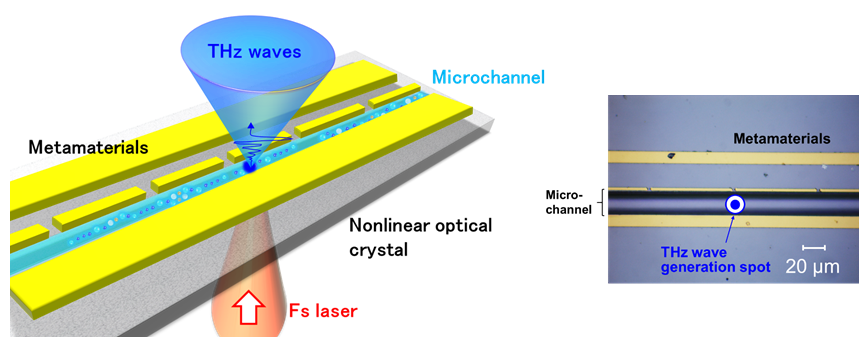
A terahertz optical spectroscopy system prototype with a sensing area comparable to the cross-sectional area of only five human hairs was developed by researchers from Osaka University’s Institute of Laser Engineering.
 Schematic diagram and photograph of the newly developed terahertz (THz) biochemical chip. The chip is made of GaAs, a nonlinear optical crystal, and is composed of five metamaterial units and a single microchannel on the surface. By irradiating with a femtosecond laser from the back surface of the crystal, a point THz light source is generated to interact with the solution. Image Credit: Kazunori Serita.
The quantity of even trace dissolved pollutants in a microscopic drop of water can be determined by monitoring the variation in peak transmittance wavelength of a terahertz radiation source. This research might result in portable sensors for purposes including monitoring water contamination, developing new drugs, and early diagnosis of diseases.
A fascinating topic of study is lab-on-a-chip technology. It is highly appealing to have portable monitoring equipment that can analyze patient samples at the patient’s bedside or track water quality outside.
However, it can be challenging to achieve great sensitivity to the concentration of target analytes of interest, particularly when samples are made up of minuscule liquid volumes.
Researchers at Osaka University have now quantified the level of trace pollution in water using a proprietary terahertz radiation source in a microfluidic device with a metamaterial structure.
Using this lab-on-a-chip system, we could detect minute changes in the concentration of trace amounts of ethanol, glucose, or minerals in water by measuring the shift in the resonance frequencies.
Kazunori Serita, Study First Author, Osaka University
The “I-design” is made up of two metallic strips, one of which has a gap of a few micrometers. It is regularly arranged in a row of five units, creating a sort of “meta-atom” whose peak optical transmittance changes depending on the amount of dissolved molecule contamination.
This gadget uses a point terahertz source technology that Osaka University previously developed. The irradiation points of a femtosecond-pulse laser beam, which causes a tightly constrained electric-field mode at the gap regions, produce a small source of terahertz light.
When the sample solution is poured into a microchannel that was constructed in the gap between the metallic strips, it changes the resonance frequency.
We succeeded in detecting just 472 attomoles of solutes in solutions with volumes of less than 100 picolitres, which is an order of magnitude better than existing microfluidic chips.
Masayoshi Tonouchi, Study Senior Author, Osaka University
This study has the potential to significantly increase portable sensing in terms of sensitivity and the quantity of liquid needed.
Journal Reference:
Serita, K., et al. (2022) I-design terahertz microfluidic chip for attomole-level sensing. Journal of Physics: Photonics. doi:10.1088/2515-7647/ac691d