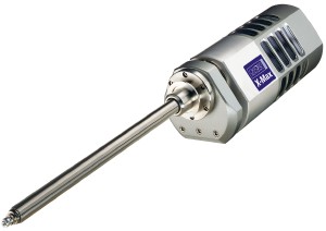
Once again, Oxford Instruments has revolutionized EDS! Its new X-Max Silicon Drift Detector (SDD) now provides electron microscopists with the biggest area detector ever - over TEN times the solid angle of conventional EDS detectors.

"This product is already changing the way people think about EDS. There is no longer a compromise between productivity and accuracy. With these new large area SDDs we are achieving world-class analysis at speeds that were inconceivable only a few years ago." Dan Varnam, New Product Introduction Director, said "This is the most exciting launch of my career. "
The X-Max Analytical SDD detector comes in a range of sizes from 20mm2 up to an outstanding 80mm2. No compromise in performance has been allowed, and the detectors achieve resolution down to 123eV with throughput far in excess of 100,000 cps (counts per second).
With a capture angle TEN times that of traditional SDDs, the new X-max can:
- Gather data 10x faster - massively increasing SEM productivity
- Gather data at 10x lower beam currents - making true nano-analysis possible on nano-scale particles and features
- Gather equivalent data in 10th of the time required by a smaller SDD - reducing the chances of sample contamination
- Run at count rates well over 100,000cps - without damaging the sample
A major advantage of the new detector is that all of these improvements come without any compromises on resolution or accurate analysis. Combined with the market-leading INCA EDS software, the system retains the analytical accuracy and usability Oxford Instruments is renowned for - only now with 10 times better productivity!
The detector has been trialled for some time with key users. Dr Phil Russell, Distinguished Professor of Physics and Science Education at Appalachian State University in the USA said "I have been working with this system for a number of months now and am very impressed with the results I have achieved on it. It provides the capability to carry out experiments I would not normally have tried to do on an SEM, and with the improved sensitivity and increased count rates allows me to investigate Nanostructured materials and devices in incredible detail. Without changing anything except my detector, I have suddenly been opened to a new world of analysis."