Oct 18 2008
By manipulating the way tiny droplets of fluid dry, Cornell researchers have created an innovative way to make and pattern nanoscale wires and other devices that ordinarily can be made only with expensive lithographic tools. The process is guided by molds that "stamp" the desired structures.
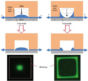
 The thickness of the gap between a mold and the surface below determines how a drop of fluid will dry. A thin gap, left, lets the droplet pull away from the edges and shrink into a nanoscale structure. A thick gap, right, pulls the droplet toward the edges to form a "corral." Although the mold is a few microns across, the result is measured in nanometers, in a process developed by Cornell professor Dan Luo and colleagues. (Luo Molecular Bioengineering Lab)
"You can in principle build almost any types of architectures you want at nanoscale," reported Dan Luo, Cornell associate professor of biological and environmental engineering, postdoctoral researcher Wenlong Cheng and colleagues. Their work is described in the online edition of the journal Nature Nanotechnology and in the October 2008 print issue.
To demonstrate the process, the researchers assembled gold nanoparticles into nanoscale wires, disks, squares, triangles and "corrals" (spaces enclosed by nanowires), and demonstrated that their nanowires could be connected to microfabricated electrodes, and through them to other circuitry. In addition to metal nanoparticles, the process could be applied to quantum dots, magnetic spheres and other nanoparticles, they said. They also assembled arrays of single salt crystals, suggesting that any material capable of crystallization could be manipulated by the process.
They began with gold nanoparticles about 12 nanometers in diameter suspended in water. To suspend metal particles in water, the researchers coated them with a "ligand" that adheres to the metal and to water. A second innovation in the Cornell process is to use single chains of synthetic DNA as the ligand. The DNA molecules extend out from the particles like hairs and, as the water evaporates, entangle the particles with one another. Adjusting the DNA lengths can precisely control the distance between the particles to make them assemble into orderly arrays called superlattices, rather than clumping together at random. Metal superlattices have applications in computer memory and photonics and have unique properties in electronic circuits.
The next step is to press down a silicone rubber mold onto a thin layer of the solution on a silicon substrate. Microscopic holes and channels in the underside of the mold effectively "stamp" the desired shapes on the fluid. As they dry, droplets shrink to create wires and other shapes measured in nanometers from a mold measured in microns. This means, the researchers say, that nanoscale superlattice features -- currently possible only with expensive, specialized equipment -- can be made in an inexpensive way.
The research was funded by the National Science Foundation under a CAREER award to Luo, and by the New York State Foundation for Science, Technology and Innovation.