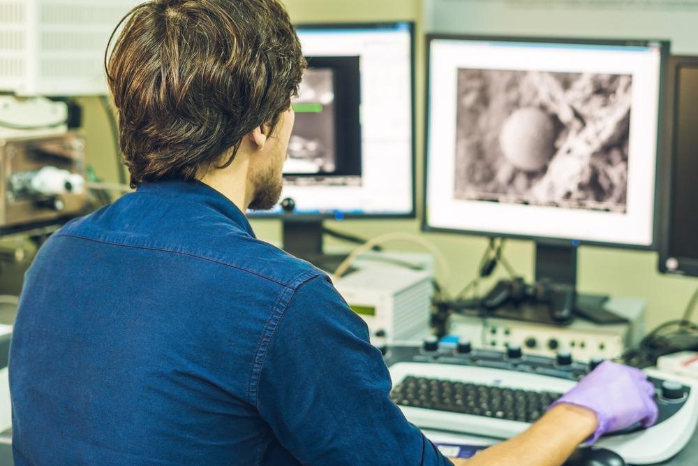
MXenes are an important recent discovery in two-dimensional (2D) materials research. Since the unique 2D material class was discovered, electron microscopy techniques have been the primary method used to investigate it. Electron microscopy can overcome the diffraction limit of conventional optical microscopy and image a sample material’s nanostructure and chemical composition at the scale of atoms.

Image Credit: Elizaveta Galitckaia/Shutterstock.com
What Are MXenes?
Graphene was the first 2D material –a material so thin that mere atoms separate either side – to come into view for materials scientists, with researchers only identifying it in the late 2000s.
The scientific community remains captivated by such materials due to their unique electronic, mechanical, optical, magnetic, and catalytic properties. Peculiar phenomena occur with these materials due to their reduced dimensionality, or 2D structure, making interactions with them behave according to the unintuitive laws of quantum mechanics.
MXenes are one of the most quickly growing fields of 2D materials research today. First discovered in 2011, MXenes are classed as layered transition metal carbides, carbonitrides, and nitrides. They are produced by layering ternary materials known as the MAX phases, for Mn+1AXn. MAX phases are a large group of hexagonal compounds assembled in layers. M represents an early transition metal, A represents an A-group element, usually aluminum, and X represents either carbon, nitrogen, or both.
The most common fabrication technique for MXenes is selective etching of the A-layers in a MAX phase to create space between the transition metal and carbon-nitrogen sheets. A hydrofluoric acid or fluoride salts with hydrochloric acid are used as an etching solvent.
How to Study MXenes
Two characterization tools have played a more important role than any others in the development of MXene research: X-ray photoelectron spectroscopy (XPS) and electron microscopy. XPS is used to study MXenes’ surface chemistry with high levels of detail, selected for its high surface sensitivity. But spatial resolution in XPS is limited to just a square micrometer in range. This means that the signal is compromised by impurities and secondary phases for powder materials.
On the other hand, electron microscopy performs well in terms of spatial resolution. For nearly a century, electron microscopy has been a fundamental tool for materials science research, with its ability to identify objects of interest and investigate them at resolutions in the nanometer (nm) range and even – in the case of (scanning) transmission electron microscopy (S)TEM – in the ångström (Å) range.
Modern electron microscopes can provide data about morphology, crystal structure, and the arrangement, composition, and chemical state of atoms simultaneously. This makes it the only technique that enables comprehensive 2D materials research at the atomic level.
Recently, environmental instruments and sample holders have progressed to the point where in situ investigations of dynamic changes of materials at atomic scales can be performed in controlled gas or liquid environments. This means researchers can move the laboratory inside an electron microscope by miniaturizing experiments. Such investigations are especially important for helping us to understand and optimize the electrochemical and catalytic performance of materials like MXenes.
SEM is Fundamental
Scanning electron microscopy (SEM) is fundamental to all materials research, and MXene studies are no exception. SEM is easily accessible and has been the main investigation method behind the rise of MXenes research in the last decade.
SEM can generate high-resolution images over five orders of magnitude in magnification. It works by rastering an electron beam across a sample, causing backscattered electrons or secondary electrons to emit and provide topographical, morphological, and microstructural information about the sample.
SEM also generates X-rays that can provide compositional data and elemental maps. SEM imaging is easy to interpret and easily conveys the potential of novel materials like MXenes. As a result, the last ten years have seen MXene images gracing the covers of numerous high-impact scientific journals.
SEM imaging confirms MXenes morphology and conversion process that starts with bulk MAX phases and finishes with a 2D MXene structure. It can also be used to verify the success of other processing methods by determining how the morphological changes from MAX bulk to MXene sheets transpired.
TEM for the Toughest Tasks
Transmission electron microscopy (TEM) is a more complicated method than SEM that requires highly trained operators and much more sample preparation. Its advantages include higher degrees of magnification and spatial resolution.
TEM transmits electrons through thin samples to provide detailed characterizations of their internal microstructures. This allows researchers to identify immediate contrast differences between different phases and the orientations of crystals in the material.
TEM was used to investigate MAX phases before MXenes were discovered.
Advanced Techniques: STEM and HAADF
While SEM and TEM are the main electron microscopy techniques used for MXene research, several specialist, advanced methods have also been brought to bear on the emerging field.
Scanning transmission electron microscopy (STEM) uses a subatomic-sized electron beam to achieve even higher resolution imaging. Cross-sectional high-angular annular dark-field (HAADF) imaging is used to determine MXenes’ crystal structure.
Continue reading: Thermal Gravimetric Analysis for MXene Research
References and Further Reading
Alnoor, H., A. Elsukova, J. Palisaitis, et al (2021). Exploring MXenes and their MAX phase precursors by electron microscopy. Materials Today Advances. Available at: https://doi.org/10.1016/j.mtadv.2020.100123.
Gogotsi, Y. and B. Anasori (2019). The rise of MXenes. ACS Nano. Available at: https://doi.org/10.1021/acsnano.9b06394.
Khan, K. et al (2020). Recent developments in emerging two-dimensional materials and their applications. Journal of Materials Chemistry C. Available at: https://doi.org/10.1039/c9tc04187g.
Novoselov, K.S., et al (2004). Electric field in atomically thin carbon. Science. Available at: https://doi.org/10.1126/science.1102896.
Disclaimer: The views expressed here are those of the author expressed in their private capacity and do not necessarily represent the views of AZoM.com Limited T/A AZoNetwork the owner and operator of this website. This disclaimer forms part of the Terms and conditions of use of this website.