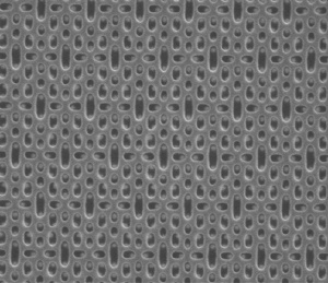
Today, IMEC presented the world's first functional 22nm CMOS SRAM cells made using EUV lithography. The 0.099µm2 SRAM cells are made with FinFETs and have both the contact and metal1 layer printed using ASML's full field extreme ultraviolet (EUV) Alpha Demo Tool (ADT). The ultra-small circuit structures were made using Applied Material's most advanced deposition systems. These results were presented during IMEC's core partner review week, which was attended - despite the economical downturn - by 250 experts representing IMEC's industrial partners in its CMOS scaling program.
 22nm SRAM array after metal1 patterning (with EUV litho) and etch
The density of the new record-breaking cells is 0.099µm², representing a 47% area scaling compared to the 0.186µm² of IMEC's 32nm cell reported last year. For the front-end-of-line process, IMEC used its high-k/metal-gate FinFET platform. The FinFETs consist of HfO2 as dielectric and TiN as metal gate and NiPt silicide for the source/drain. The minimum active FIN pitch is 90nm. The FinFET layers were printed using ASML's 1900i immersion lithography tools. The metallization of the contact holes was realized using Applied Materials most advanced contact processing modules for inter-layer barrier Ti and TiN before tungsten fill and chemical mechanical polishing.
Compared to the 32nm cell, where only the contact holes were printed with the EUV tool, IMEC now used ASML's ADT to pattern both the contact with a size of ~45nm and metal1 layers (60nm width and 46nm spaces). The results show a good overlay performance. And the single patterning approach further strengthens the case for EUV as a cost-effective solution.
Luc Van den hove, Chief Operating Officer at IMEC: "Our successful fabrication of 22nm SRAM cells with EUV is an important milestone, both for the development of 22nm processes, and for the roadmap of EUV lithography. This SRAM cell integration shows that EUV photo process technology is making excellent progress as a cost-effective single patterning approach. We believe that EUV remains a candidate for use in the later stages of the 22nm technology.
Luc Van den hove further comments: "Key to the success of our research is the presence at IMEC of leading tool suppliers allowing us to use the most advanced tools, the collaborative research of our staff and the on-site residents from IDMs, foundries, equipment and material suppliers, and the support and funding of the EC program PULLNANO. With such concerted collaborations, the semiconductor industry is able to keep innovating and to follow Moore's momentum."
In its core program, IMEC works together with leading IC companies on future CMOS technologies. Key partners in 2009 are Intel, Micron, Panasonic, Samsung, TSMC, Elpida, Hynix, Powerchip, Infineon, NXP, Qualcomm, Sony, ST Microelectronics.