Jun 17 2009
A simulation of electrical current moving through a futuristic electronic transistor has been modeled atom-by-atom in less than 15 minutes by Purdue University researchers.
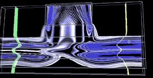
 Purdue researchers have performed a complete atom-by-atom simulation of current passing through an experimental transistor in just 15 minutes using Jaguar, the world's second fastest computer. The 38,000-atom simulation was of an experimental indium gallium arsenide-based transistor developed at the Massachusetts Institute of Technology. The image here shows the current flow through a different but related simulation. (Purdue University animation/Gerhard Klimeck)
The work demonstrates that future electronic devices can be quickly simulated on advanced computers, opening the door to new nanoscale semiconductor components that are more powerful and use less energy.
The simulation was run on Oak Ridge National Laboratory's Jaguar supercomputer, the world's second fastest and one of just two computers capable of petascale performance.
The modeling of the transistor ran on more than 147,000 computer processors simultaneously, according to Gerhard Klimeck, professor of electrical and computer engineering and director for the National Science Foundation-funded Network for Computational Nanotechnology.
"If this had run on a single-processor computer it would have taken us 3.3 years to complete," Klimeck said. "This is the first time we've been able to do an atomic-level simulation of a transistor within the realm of engineering instead of as a once-in-a-lifetime computer run."
The transistor simulation represented 38,000 atoms and examined the current that passes through the experimental transistor.
Being able to model semiconductors and transistors atom-by-atom is important. As electronic components approach nanoscale they begin behaving quite differently because of quantum effects, and because of what scientists call "atomic granularity," which means that devices built atom-by-atom break apart instead of the surface of the device wearing down.
Despite the different behaviors of nanoelectronics, most simulations of these devices ignore quantum and atomistic effects primarily because engineers believe that such simulations are too difficult and expensive.
Mathieu Luisier, an assistant research professor in Purdue's Birck Nanotechnology Center and the National Science Foundation's Network for Computational Nanotechnology, says the Jaguar simulation shows that with the advent of petascale computing, that is no longer the case.
"Many people still believe this is computationally too expensive and limited to unrealistically small structures," Luisier says. "But full-machine runs on supercomputers like Jaguar make it now possible to perform simulations of already manufactured transistors. In a near future I can imagine running nanoscale design jobs on large supercomputers like Jaguar on a daily basis."
The simulation was run using OMEN, a nanoelectronics modeling tool developed by Luisier while at the Swiss Federal Institute of Technology Zurich. (OMEN-based simulation tools also are available at no cost at http://www.nanoHUB.org)
"The problem with existing modeling and simulation tools is that as device structures get smaller, these tools quickly reach a limit of countable atoms within the structure, and the standard simulation tool breaks down," Klimeck says. "You are left with no information about the local arrangement of the atoms on the device, distortions due to strain or the quantum effects.
"Having a model that understands all of that is critical to the development of future semiconductors."
The experimental transistor modeled on Jaguar uses the semiconductor material indium gallium arsenide in place of silicon and was developed at the Massachusetts Institute of Technology by Jesús A. del Alamo, a professor of electrical engineering.
Del Alamo says there is a need for faster development of new electronic components.
"The search for a replacement technology for silicon semiconductors is one of the greatest technical challenges of our time," del Alamo says. "The demonstration by Purdue of a very fast and massively parallel simulation for nanometer-scale transistors involving very complex physics is extremely significant because it enables the quick exploration of different device designs. This allows us to focus our experimental efforts on the designs that offer the greatest potential for future devices."
Jaguar, the supercomputer that enabled this work, ranks second on the bi-annual Top500.org list of supercomputers and was built using 182,000 AMD Opteron processors. Computers of this size and scale open new doors to research, says Douglas Kothe, director of science at the National Center for Computational Science, which is based at Oak Ridge National Laboratory.
"Professor Klimeck and his colleague have demonstrated the unique transformational scientific opportunity that comes from scaling a science application to fully exploit the capabilities of petascale systems like the Cray XT5 at the Oak Ridge Leadership Computing Facility," Kothe says.