Jul 28 2009
Shin-Etsu MicroSi has introduced an extension of their photosensitive dry film dielectric technology for 3D Through-Silicon Vias and two-dimensional wafer bonding applications. This SINR negative photoresist film, introduced last year, is available now in thicknesses from 12 to 100 microns. Other non-3D applications for the photoresist include stress buffer and RDL dielectrics for wafer-level packaging.
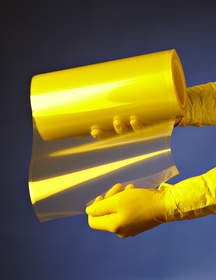 Shin-Etsu MicroSi's dry film photoresist
These films feature:
- Low residual stress featuring an ultra low modulus, which produces a "rubbery" consistency to the film and results in minimal wafer bow, particularly important with 300mm wafers that are hard to process if the wafers are not flat.
- Low temperature cure: many device types, for example, can fail if processed above 200° C.
- Good adhesion: Shin-Etsu proprietary adhesion promoters are built in to ensure good bonding.
- Low dielectric constant for superior electrical performance.
Shin-Etsu Chemical developed the siloxane-based SINR series photoresist from their long tradition of working with silicone materials. Shin-Etsu has tailored the materials to specific, custom applications.
Through-Silicon Vias (TSV)
For TSV applications, these films can be applied with a roll laminator or by vacuum lamination, which is preferred for TSV because the combination of temperature, pressure and vacuum allows the material to flow into the vias, producing a void-free dielectric fill and a planarized surface. CMOS image sensors are the first process that now uses this TSV technology. TSVs can typically feature vias that are 50 to 100 microns across.
CMOS Image Sensors:
Shin-Etsu MicroSi SINR works well for bonding applications including:
- Wafer-to-wafer
- Chip-to-wafer
- Wafer-to-glass, as in CMOS image sensors
The SINR 3170 series and SINR 3570 series are now in production and available for sampling and evaluation by contacting Shin-Etsu MicroSi.