Oct 23 2009
A team of engineers from the University of Pennsylvania has transformed simple nanowires into reconfigurable materials and circuits, demonstrating a novel, self-assembling method for chemically creating nanoscale structures that are not possible to grow or obtain otherwise.
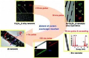
 Using only chemical reactants, engineers transformed semiconducting nanowires into a variety of useful, nanoscale materials. Credit: Ritesh Agarwal, the University of Pennsylvania
The research team, using only chemical reactants, transformed semiconducting nanowires into a variety of useful, nanoscale materials including nanoscale metal strips with periodic stripes and semiconducting patterns, purely metallic nanowires, radial heterostructures and hollow semiconducting nanotubes in addition to other morphologies and compositions.
Researchers used ion exchange, one of the two most common techniques for solid phase transformation of nanostructures. Ion (cation/anion) exchange reactions exchange positive or negative ions and have been used to modify the chemical composition of inorganic nanocrystals, as well as create semiconductor superlattice structures. It is the chemical process, for example, that turns hard water soft in many American households.
Future applications of nanomaterials in electronics, catalysis, photonics and bionanotechnology are driving the exploration of synthetic approaches to control and manipulate the chemical composition, structure and morphology of these materials. To realize their full potential, it is desirable to develop techniques that can transform nanowires into tunable but precisely controlled morphologies, especially in the gas-phase, to be compatible with nanowire growth schemes. The assembly, however, is an expensive and labor-intensive process that prohibits cost-effective production of these materials.
Recent research in the field has enabled the transformation of nanomaterials via solid-phase chemical reactions into nonequilibrium, or functional structures that cannot be obtained otherwise.
In this study, researchers transformed single-crystalline cadmium sulfide nanowires into composition-controlled nanowires, core-shell heterostructures, metal-semiconductor superlattices, single-crystalline nanotubes and metallic nanowires by utilizing size-dependent cation-exchange reactions along with temperature and gas-phase reactant delivery control. This versatile, synthetic ability to transform nanowires offers new opportunities to study size-dependent phenomena at the nanoscale and tune their chemical/physical properties to design reconfigurable circuits.
Researchers also found that the speed of the cation exchange process was determined by the size of the starting nanowire and that the process temperature affected the final product, adding new information to the conditions that affect reaction rates and assembly.
"This is almost like magic that a single-component semiconductor nanostructure gets converted into metal-semiconductor binary superlattice, a completely hollow but single crystalline nanotube and even a purely metallic material," said Ritesh Agarwal, assistant professor in the Department of Materials Science and Engineering at Penn. "The important thing here is that these transformations cannot take place in bulk materials where the reaction rates are incredibly slow or in very small nanocrystals where the rates are too fast to be precisely controlled. These unique transformations take place at 5-200 nanometer-length scales where the rates can be controlled very accurately to enable such intriguing products. Now we are working with theoreticians and designing new experiments to unravel this 'magic' at the nanoscale."
The fundamental revelation in this study is a further clarification of nanoscale chemical phenomena. The study also provides new data on how manufacturers can assemble these tiny circuits, electrically connecting nanoscale structures through chemical self-assembly.
It also opens up new possibilities for the transformation of nanoscale materials into the tools and circuits of the future, for example, self-assembling nanoscale electrical contacts to individual nanoscale components, smaller electronic and photonic devices such as a series of electrically connected quantum dots for LEDs or transistors, as well as improved storage capacities for batteries.
More information: The study has been published in the current issue of the journal Nano Letters.