Nov 10 2009
Purdue University researchers are making progress in developing a new type of transistor that uses a finlike structure instead of the conventional flat design, possibly enabling engineers to create faster and more compact circuits and computer chips.
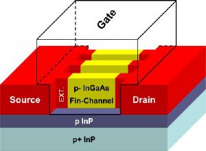
 Researchers are making progress in developing new types of transistors, called finFETs, which use a finlike structure instead of the conventional flat design, possibly enabling engineers to create faster and more compact circuits and computer chips. The fins are made not of silicon, but from a material called indium-gallium-arsenide, as shown in this illustration. Credit: Birck Nanotechnology Center, Purdue University
The fins are made not of silicon, like conventional transistors, but from a material called indium-gallium-arsenide. Called finFETs, for fin field-effect-transistors, researchers from around the world have been working to perfect the devices as potential replacements for conventional transistors.
In work led by Peide Ye, an associate professor of electrical and computer engineering, the Purdue researchers are the first to create finFETs using a technology called atomic layer deposition. Because atomic layer deposition is commonly used in industry, the new finFET technique may represent a practical solution to the coming limits of conventional silicon transistors.
"We have just demonstrated the proof of concept here," Ye said.
Findings are detailed in three research papers being presented during the International Electron Devices Meeting on Dec. 7-9 in Baltimore. The work is led by doctoral student Yanqing Wu, who provided major contributions for two of the papers.
The finFETs might enable engineers to sidestep a problem threatening to derail the electronics industry. New technologies will be needed for industry to keep pace with Moore's law, an unofficial rule stating that the number of transistors on a computer chip doubles about every 18 months, resulting in rapid progress in computers and telecommunications. Doubling the number of devices that can fit on a computer chip translates into a similar increase in performance. However, it is becoming increasingly difficult to continue shrinking electronic devices made of conventional silicon-based semiconductors.
In addition to making smaller transistors possible, finFETs also might conduct electrons at least five times faster than conventional silicon transistors, called MOSFETs, or metal-oxide-semiconductor field-effect transistors.
"The potential increase in speed is very important," Ye said. "The finFETs could enable industry to not only create smaller devices, but also much faster computer processors."
Transistors contain critical components called gates, which enable the devices to switch on and off and to direct the flow of electrical current. In today's chips, the length of these gates is about 45 nanometers, or billionths of a meter.
The semiconductor industry plans to reduce the gate length to 22 nanometers by 2015. However, further size reductions and boosts in speed are likely not possible using silicon, meaning new designs and materials will be needed to continue progress.
Indium-gallium-arsenide is among several promising semiconductor alloys being studied to replace silicon. Such alloys are called III-V materials because they combine elements from the third and fifth groups of the periodical table.
Creating smaller transistors also will require finding a new type of insulating layer essential for the devices to switch off. As gate lengths are made smaller than 22 nanometers, the silicon dioxide insulator used in conventional transistors fails to perform properly and is said to "leak" electrical charge.
One potential solution to this leaking problem is to replace silicon dioxide with materials that have a higher insulating value, or "dielectric constant," such as hafnium dioxide or aluminum oxide.
The Purdue research team has done so, creating finFETs that incorporate the indium-gallium-arsenide fin with a so-called "high-k" insulator. Previous attempts to use indium-gallium-arsenide finFETs to make devices have failed because too much current leaks from the circuit.
The researchers are the first to "grow" hafnium dioxide onto finFETs made of a III-V material using atomic layer deposition. The approach could make it possible to create transistors using the thinnest insulating layers possible - only a single atomic layer thick.
The finlike design is critical to preventing current leakage, in part because the vertical structure can be surrounded by an insulator, whereas a flat device has the insulator on one side only.