Jan 7 2010
Nanoscience has the potential to play an enormous role in enhancing a range of products, including sensors, photovoltaics and consumer electronics. Scientists in this field have created a multitude of nano scale materials, such as metal nanocrystals, carbon nanotubes and semiconducting nanowires.
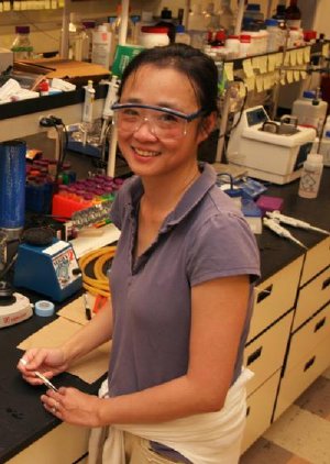
 Jen Cha, a UC San Diego nanoengineering professor, is pushing the envelop in nanoscience by using biology to engineer the assembly of nanoscale materials for applications in medicine, electronics and energy. Credit: UC San Diego
However, despite their appeal, it has remained an astounding challenge to engineer the orientation and placement of these materials into the desired device architectures that are reproducible in high yields and at low costs – until now. Jen Cha, a UC San Diego nanoengineering professor, and her team of researchers, have discovered that one way to bridge this gap is to use biomolecules, such as DNA and proteins. Details of this discovery were recently published in a paper titled "Large Area Spatially Ordered Arrays of Gold Nanoparticles Directed by Lithographically Confined DNA Origami," in Nature Nanotechology.
"Self-assembled structures are often too small and affordable lithographic patterns are too large," said Albert Hung, lead author of the Nature Nanotechnology paper and a post doc working in Cha's lab. "But rationally designed synthetic DNA nanostructures allow us to access length scales between 5 and 100 nanometers and bridge the two systems.
"People have created a huge variety of unique and functional nanostructures, but for some intended applications they are worthless unless you can place individual structures, billions or trillions of them at the same time, at precise locations," Hung added. "We hope that our research brings us a step closer to solving this very difficult problem."
Hung said the recently discovered method may be useful for fabricating nanoscale electronic or optical circuits and multiplex sensors.
"A number of groups have worked on parts of this research problem before, but to our knowledge, we're the first to attempt to address so many parts together as a whole," he said.
One of the main applications of this research that Cha and her group are interested in is for sensing. "There is no foreseeable route to be able to build a complex array of different nanoscale sensing elements currently," said Cha, a former IBM research scientist who joined the UCSD Jacobs School of Engineering faculty in 2008. "Our work is one of the first clear examples of how you can merge top down lithography with bottom up self assembly to build such an array. That means that you have a substrate that is patterned by conventional lithography, and then you need to take that pattern and merge it with something that can direct the assembly of even smaller objects, such as those having dimensions between 2 and 20 nanometers. You need an intermediate template, which is the DNA origami, which has the ability to bind to something else much smaller and direct their assembly into the desired configuration. This means we can potentially build transistors from carbon nanotubes and also possibly use nanostructures to detect certain proteins in solutions. Scientists have been talking about patterning different sets of proteins on a substrate and now we have the ability to do that."
Cha said the next step would be to actually develop a device based on this research method.
"I'm very interested in the applications of this research and we're working our way to get there," she said.
For the last 6 years, Cha's research has focused on using biology to engineer the assembly of nanoscale materials for applications in medicine, electronics and energy. One of the limitations of nanoscience is it doesn't allow mass production of products, but Cha's work is focused on trying figure out how to do that and do it cheaply. Much of her recent work has focused on using DNA to build 2D structures.
"Using DNA to assemble materials is an area that many people are excited about," Cha said. "You can fold DNA into anything you want – for example, you can build a large scaffold and within that you could assemble very small objects such as nano particles, nano wires or proteins.
"Engineers need to understand the physical forces needed to build functional arrays from functional materials," she added. "My job as a nanoengineer is to figure out what you need to do to put all the different parts together, whether it's a drug delivery vehicle, photovoltaic applications, sensors or transistors. We need to think about ways to take all the nano materials and engineer them it into something people can use and hold."
Large-area spatially ordered arrays of gold nanoparticles directed by lithographically confined DNA origami, Nature Nanotechnology, Albert M. Hung, Christine M. Micheel, Luisa D. Bozano, Lucas W. Osterbur, Greg M. Wallraff2 & Jennifer N. Cha