Jan 22 2010
Watch a gecko walk up a wall. It defies gravity as it sticks to the surface no matter how smooth it appears to be.

What's happening isn't magic. The gecko stays put because of the electrical attraction - the van der Waals force - between millions of microscopic hairs on its feet and the surface.
The principle applies to new research at Rice University reported this week in the online version of the journal ACS Nano. But in this case, the hairs figuratively come off the gecko and plant themselves on the wall.
Rice graduate student Cary Pint has come up with a way to transfer patterns of strongly aligned, single-walled carbon nanotubes (SWNTs) from a substrate to another surface - any surface - in a matter of minutes. The same substrate, with its catalyst particles still intact, can repeatedly be used to grow more nanotubes, almost like inking a rubber stamp.
Pint is primary author of the research paper, which also details a way to quickly and easily determine the range of diameters in a batch of nanotubes grown through chemical vapor deposition (CVD). Common spectroscopic techniques are poor at seeing tubes bigger than two nanometers in diameter - or most of the nanotubes in the CVD "supergrowth" process.
"This is important since all of the properties of the nanotubes - electrical, thermal and mechanical - change with diameter," he said. “The best thing is that nearly every university has an FTIR (Fourier transform infrared) spectrometer sitting around that can do these measurements, and that should make the process of synthesis and application development from carbon nanotubes much more precise."
Pint and other students and colleagues of Robert Hauge, a Rice distinguished faculty fellow in chemistry, are also investigating ways to take printed films of SWNTs and make them all-conducting or all-semiconducting - a process Hauge refers to as "Fermi-level engineering" for its ability to manipulate electron movement at the nanoscale.
Combined, the techniques represent a huge step toward a nearly limitless number of practical applications that include sensors, highly efficient solar panels and electronic components.
"A big frontier for the field of nanoscience is in finding ways to make what we can do on the nanoscale impact our everyday activities," Hauge said. "For the use of carbon nanotubes in devices that can change the way we do things, a straightforward and scalable way of patterning aligned carbon nanotubes over any surface and in any pattern is a major advance."
Pint said an afternoon of "experimenting with creative ideas" as a first-year graduate student turned into a project that held his interest through his time at Rice. "I realized early on it may be useful to transfer carbon nanotubes to other surfaces," he said.
"I started playing around with water vapor to clean up the amorphous carbons on the nanotubes. When I pulled out a sample, I noticed the nanotubes actually stuck to the tweezers.
"I thought to myself, 'That's really interesting ...'"
Water turns out to be the key. After growing the nanotubes, Pint etches them with a mix of hydrogen gas and water vapor, which weakens the chemical bonds between the tubes and the metal catalyst. When stamped, the nanotubes lay down and adhere, via van der Waals, to the new surface, leaving all traces of the catalyst behind.
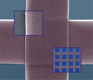
Pint, who hopes to defend his dissertation in August, developed a steady enough hand to deposit nanotubes on a range of surfaces - "anything I could lay my hands on" - in patterns that could easily be replicated and certainly enhanced by industrial processes. A striking example of his work is a crisscross film of nanotubes made by stamping one set of lines onto a surface and then reusing the catalyst to grow more tubes and stamping them again over the first pattern at a 90-degree angle. The process took no more than 15 minutes.
"I'll be honest - that was a little bit of luck, combined with the skill of having done this for a few years," he said of the miniature work of art. "But if I were in industry, I would make a machine to do this for me."
Pint believes industries will take a hard look at the technique, which he said could be scaled up easily, for embedding nanotube circuitry into electronic devices.
His own goal is to develop the process to make a range of highly efficient optical-sensing devices. He's also investigating doping techniques that will take the guesswork out of growing metallic (conducting) or semiconducting SWNTs.