Jan 27 2010
A bizarre substance predicted to shrink electronics and give quantum physicists a new tabletop toy behaves pretty much as its designers expected.
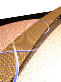
 Image courtesy Hailin Peng.
Last month in Nature Materials, SLAC researchers and their coworkers at Stanford confirmed how electric current moves on tiny ribbons of topological insulator—a material that insulates in its bulk but conducts unusually well on the surface. The work came out of a close collaboration between the research groups of Stanford researcher Yi Cui, and Zhi-Xun Shen and Shoucheng Zhang of the Stanford Institute for Materials and Energy Science.
"Electrical current properties are very difficult to study in a typical bulk sample of these topological insulators," said Shen, director of SIMES, a joint Stanford/SLAC institute. "By making very small nanoribbons we were able to study the unique surface properties."
In extremely thin ribbons of the compound bismuth selenide, the large ratio of edges to innards makes the material's coolest properties easy to detect. Electrons running on the nanoribbon surface flow especially smoothly, act as though they have no mass, and have a set spin—at least when the ribbons are immersed in frigid liquid helium. In principle, the properties could extend to room temperature.
"It opens up a lot of future applications," said SIMES physicist and co-author Yulin Chen. The material could be a boon to spintronics, a technology that uses electron spin to store information. The applications of spintronics include minuscule computer chips and sensors, and quantum computing.
But applications are just part of the substance's appeal. Because of their unique surface properties, the ribbons open new testing ground for physics theories, said co-author Keji Lai, a postdoctoral scholar in Shen's group. The "explosion" of research articles on the topic since these exotic properties were predicted in 2006 speaks to the physicists' excitement.
"We can actually play with table top systems and understand very high level quantum mechanics," Lai said. "This [new result] really paves the way to do that kind of experiment."
The work grew out of a casual conversation between Lai and materials scientist Hailin Peng, previously in the Cui group at the Stanford Department of Materials Science and Engineering and now on faculty at Peking University, China.
"I chatted with him over lunch and told him this family of interesting materials," Lai said. "He came back the next day and said they have an idea how to build them and make them very thin. One week later, he showed me electron microscope images of these materials in ribbon form."
Peng, along with Cui's graduate students Desheng Kong and Stefan Meister, used a well-known technique called "Vapor-Liquid-Solid Synthesis" to grow the ribbons. Bismuth selenide vapor reacts under low pressure and furnace heat with specially prepared gold nanoparticles to form tiny liquid droplets. Once saturated, the liquid begins to sprout solid bismuth selenide ribbons, each attached to a gold particle. The diameter of the gold particles dictates the thickness of the nanoribbons.
Making the nanoribbons thinner and thinner—until they are practically all surface—may be the key to seeing their outlandish behavior at room temperature. According to Stanford materials scientist Yi Cui, who still collaborates with Peng, they can now make nanoribbons that are merely 10 atoms thick-- 25 times thinner than those described in December's article.
At such small distances, electrons on the top and bottom of the nanoribbons can cross-talk, according to predictions by coauthors and SIMES researchers Zhang and Xiaoliang Qi. Only theory has explored the bizarre behaviors this communication would cause.
"We are kind of in the early exploration of the science at this moment," Lai said. "In the early days of semiconductors people spent a lot of time just understanding the fundamental science. Once they laid out the physical properties of these materials, the engineers were very powerful at building complicated structures and bringing them to every-day life."
Both Lai and Chen would like to see more materials scientists and engineers pitching in.
"Our job is to motivate and inspire more people to join the field," Chen said. "The more people join this field the faster the progress can be."