Jun 16 2010
To advance its work in next-generation 3D semiconductor integration, the newly opened All Silicon System Integration Dresden (ASSID), a leading-edge microelectronic packaging and system integration center run by the Fraunhofer IZM Institute, has ordered a 300 mm AltaCVD system from equipment supplier Altatech Semiconductor S.A.
This is the fourth order for AltaCVD equipment from a major research laboratory.
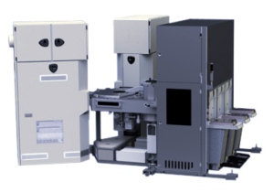
 300 mm AltaCVD system
ASSID will use the AltaCVD system to create through silicon vias (TSV), critical features in 3D semiconductor integration. Processing both standard and thin silicon wafers, the low-temperature AltaCVD tool will deposit stacks of film layers and ultrathin, conformal isolation layers inside deep vias and trenches with aspect ratios as high as 40:1.
In addition to handling either 200 mm or 300 mm wafers, AltaCVD's flexible architecture allows it to be used in volume production for plasma-enhanced deposition (PECVD) of dielectric materials, stacks and metal films as well as in R&D for metal-organic processing (MOCVD) in back-end-of-line (BEOL) applications such as creating direct-platable barriers.
"ASSID's order confirms that our platform, chambers and processes are fulfilling today's most demanding requirements for advanced materials deposition," said Jean-Luc Delcarri, president of Altatech Semiconductor. "Our low-temperature processing and innovative vaporization technology for liquid precursors makes AltaCVD uniquely qualified to deposit the films required for TSV and microsystems integration."
The equipment is scheduled to go online in the third quarter of this year at ASSID's facility in Dresden. The site's Class 1,000 cleanroom is equipped with a complete 300 mm wafer fabrication line for TSV formation and post-processing on both the frontside and backside of wafers, wafer thinning, 3D device stacking, and package assembly and testing.
Source: http://www.altatech-sc.com/