Jul 30 2010
What researchers might call "white graphene" may be the perfect sidekick for the real thing as a new era unfolds in nanoscale electronics.
But single-atom-thick layers of hexagonal boron nitride (h-BN), the material under intense study at Rice University's world-class Department of Mechanical Engineering and Materials Science, are likely to find some macro applications as well.
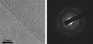
 A transmission electron microscope image, left, shows one-atom-thick layers of hexagonal boron nitride edge-on. At right is a selected area electron diffraction of an h-BN layer.
Researchers in the lab of Pulickel Ajayan, Rice's Benjamin M. and Mary Greenwood Anderson Professor in Mechanical Engineering and Materials Science and of chemistry, have figured out how to make sheets of h-BN, which could turn out to be the complementary apple to graphene's orange.
The results were reported last week in the online journal Nano Letters.
Graphene, touted as a possible successor to silicon in microelectronics applications, is the new darling of research labs that hope to take advantage of its superb electronic properties.
Hexagonal boron nitride, on the other hand, is an insulator. Earlier this year, Rice postdoctoral researchers in Ajayan's group found a way to implant islands of h-BN into sheets of graphene, a unique way to exert a level of control over the sheet's electronic character.
Now the team, led by primary author Li Song, has figured out how to deposit sheets of pure h-BN, which is naturally white in bulk form, anywhere from one to five atoms thick on a copper substrate. The material can then be transferred to other substrates.
They used a chemical vapor deposition process to grow the h-BN sheets on a 5-by-5 centimeter copper backing at temperatures around 1,000 degrees Celsius. The sheets could then be stripped from the copper and placed on a variety of substrates.
Ultimately, Song sees h-BN sheets finding wide use as a highly effective insulator in graphene-based electronics, another stride on the quick-step march toward the replacement of silicon with materials that could push beyond the boundaries of Moore's Law, which states the number of transistors that can be placed on an integrated circuit doubles about every two years.
He said it should be also possible to draw microscopic patterns of graphene and h-BN, which could be useful in creating nanoscale field-effect transistors, quantum capacitors or biosensors.
Strength tests using the tip of an atomic force microscope to push h-BN into holes in a silicon substrate showed it to be highly elastic and nearly as strong as graphene, the single-atom form of pure carbon.
Song said the size of h-BN sheets is limited only by the size of the copper foil and furnace used to grow it. The process should be adaptable to the same kind of roll-to-roll technique recently used to form 30-inch sheets of graphene. "If you have a huge furnace, you can go large," he said.
Source: http://media.rice.edu/