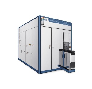
Applied Materials, Inc. today announced its Applied Aera3™ Mask Inspection system, enabling photomask and chip manufacturers to meet the most critical defect detection challenges for all photomasks at 22nm, using its proven aerial imaging technology.
Building on the groundbreaking Applied Aera2 system, the new system improves detection sensitivity by 50%, enabling inspection of smaller circuit features while boosting its unique ability to classify mask defects according to their impact on the wafer. This key benefit makes the Aera3 system the fastest, most accurate mask qualification solution available.
 Applied Materials introduced its Aera3 system for inspecting advanced 22nm and EUV photomasks using proven aerial imaging technology.
Today’s advanced lithography uses double-patterning (DP) and source-mask optimization (SMO) techniques where the features on the mask bear almost no resemblance to the final pattern on the printed wafer. Conventional high resolution inspection systems use models to simulate the projected mask image on the wafer and have difficulty determining which defects are important. The Aera3 system’s enhanced aerial imaging technology emulates the optical system of the lithography scanner, allowing users to immediately see if a defect will cause problems or can safely be ignored.
The Aera3 system introduces multiple innovations that combine to improve detection sensitivity, including a more powerful light source, smaller pixel size, sophisticated illumination shaping and polarization. In addition, the Aera3 is the first system capable of inspecting extreme ultraviolet lithography (EUVL) masks using illumination shaping. This contrast-enhancing technology, coupled with ultra-small 67nm pixel size, enables the optional EUVL module to detect defects as small as 12nm, making the Aera3 system the ideal tool to support customers’ pathfinding EUVL development.
“The Aera3 system’s benchmark capabilities are a result of our close collaboration with cutting-edge mask shops around the world,” said Ronen Benzion, vice president and general manager of Applied’s Process Diagnostics and Control division. “The system addresses all inspection applications for next generation masks, making it an essential tool to rapidly qualify new masks and to track mask quality over time, bringing productivity gains to the entire lithography cell.”
Applied Materials will showcase the Aera3 system at the 2010 SPIE Photomask Technology conference and exhibition being held in Monterey, California.
Source: http://www.appliedmaterials.com/