The ability of phase-change materials to readily and swiftly transition between different phases has made them valuable as a low-power source of non-volatile or “flash” memory and data storage.
Now an entire new class of phase-change materials has been discovered by researchers with the Lawrence Berkeley National Laboratory (Berkeley Lab) and the University of California (UC) Berkeley that could be applied to phase change random access memory (PCM) technologies and possibly optical data storage as well. The new phase-change materials – nanocrystal alloys of a metal and semiconductor – are called “BEANs,” for binary eutectic-alloy nanostructures.
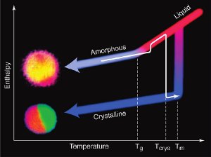
 This schematic shows enthalpy curves sketched for the liquid, crystalline and amorphous phases of a new class of nanomaterials called “BEANs” for Binary Eutectic-Alloy Nanostructures. (Image courtesy of Daryl Chrzan)
“Phase changes in BEANs, switching them from crystalline to amorphous and back to crystalline states, can be induced in a matter of nanoseconds by electrical current, laser light or a combination of both,” says Daryl Chrzan, a physicist who holds joint appointments with Berkeley Lab’s Materials Sciences Division and UC Berkeley’s Department of Materials Science and Engineering. “Working with germanium tin nanoparticles embedded in silica as our initial BEANs, we were able to stabilize both the solid and amorphous phases and could tune the kinetics of switching between the two simply by altering the composition.”
Chrzan is the corresponding author on a paper reporting the results of this research which has been published in the journal NanoLetters titled “Embedded Binary Eutectic Alloy Nanostructures: A New Class of Phase Change Materials.”
Co-authoring the paper with Chrzan were Swanee Shin, Julian Guzman, Chun-Wei Yuan, Christopher Liao, Cosima Boswell-Koller, Peter Stone, Oscar Dubon, Andrew Minor, Masashi Watanabe, Jeffrey Beeman, Kin Yu, Joel Ager and Eugene Haller.
“What we have shown is that binary eutectic alloy nanostructures, such as quantum dots and nanowires, can serve as phase change materials,” Chrzan says. “The key to the behavior we observed is the embedding of nanostructures within a matrix of nanoscale volumes. The presence of this nanostructure/matrix interface makes possible a rapid cooling that stabilizes the amorphous phase, and also enables us to tune the phase-change material’s transformation kinetics.”
A eutectic alloy is a metallic material that melts at the lowest possible temperature for its mix of constituents. The germanium tin compound is a eutectic alloy that has been considered by the investigators as a prototypical phase-change material because it can exist at room temperature in either a stable crystalline state or a metastable amorphous state. Chrzan and his colleagues found that when germanium tin nanocrystals were embedded within amorphous silica the nanocrystals formed a bilobed nanostructure that was half crystalline metallic and half crystalline semiconductor.
“Rapid cooling following pulsed laser melting stabilizes a metastable, amorphous, compositionally mixed phase state at room temperature, while moderate heating followed by slower cooling returns the nanocrystals to their initial bilobed crystalline state,” Chrzan says. “The silica acts as a small and very clean test tube that confines the nanostructures so that the properties of the BEAN/silica interface are able to dictate the unique phase-change properties.”
While they have not yet directly characterized the electronic transport properties of the bilobed and amorphous BEAN structures, from studies on related systems Chrzan and his colleagues expect that the transport as well as the optical properties of these two structures will be substantially different and that these difference will be tunable through composition alterations.
“In the amorphous alloyed state, we expect the BEAN to display normal, metallic conductivity,” Chrzan says. “In the bilobed state, the BEAN will include one or more Schottky barriers that can be made to function as a diode. For purposes of data storage, the metallic conduction could signify a zero and a Schottky barrier could signify a one.”
Chrzan and his colleagues are now investigating whether BEANs can sustain repeated phase-changes and whether the switching back and forth between the bilobed and amorphous structures can be incorporated into a wire geometry. They also want to model the flow of energy in the system and then use this modeling to tailor the light/current pulses for optimum phase-change properties.
The in-situ Transmission electron microscopy characterizations of the BEAN structures were carried out at Berkeley Lab’s National Center for Electron Microscopy, one of the world’s premier centers for electron microscopy and microcharacterization.