Sep 17 2010
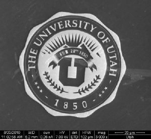
In an example of how a technology wonk displays school spirit, an engineer has created a golden University of Utah logo that is smaller than the width of an average human hair.
The gold etching is only 70 microns across - that's 70 millionths of a meter, or less than three one-thousandths of an inch, which is about the diameter of a blonde hair, among the thinnest types of human hair.
 This electron microscope image shows a gilded University of Utah medallion -- one of several official symbols and logos for the university -- that measures only 70 microns across, which is about the diameter of a single blonde human hair. The medallion is magnified 3,000 times in this image. The gold-covered parts of the medallion appear white, while the silicon background is dark. The medallion was made using a process called electron-beam lithography. It was created by Randy Polson, a senior optical engineer at the university's Department of Physics and Astronomy, as part of his job adjusting the microscope for use by researchers and private businesses. Photo Credit: Randy Polson, The University of Utah
The etching was done on a silicon base using a thin beam of electrons from one of two electron microscopes bought by the university in 2008. While the technique of electron-beam lithography is not new, the medallion symbol is more complex than the patterns commonly made.
"People usually do things like lines and rectangles," says Randy Polson, who made the tiny medallion and is a senior optical engineer for the university's Department of Physics and Astronomy. "The software that came with the microscope included some stick-figure demos. I thought, 'Hey, I can do better than a stick figure.'"
The medallion is one of several official logos used by the university. It depicts the university's block U symbol and founding date, with a background of mountains and rays of sunshine.
It is engraved on a chip of silicon two-fifths of an inch square. To the naked eye it is a barely discernable speck. Under a conventional light microscope, it looks like a fuzzy circle. Its full detail is revealed only by a scanning electron microscope - the same device that was used to create it.
In the electron microscope image, the gold-covered parts appear white, while the silicon background appears black. The finest line on the medallion encircles the design. That line is a mere 20 nanometers thick. That's 20 billionths of a meter, or about eight ten-millionths of an inch wide. That is the length of chain of 75 gold atoms, Polson says.
Scanning electron microscopes are used most often to visualize the surface structure of objects. The microscope sends a thin beam of electrons onto the specimen, scanning back and forth over the surface.
The most common imaging mode detects "secondary electrons" released from the specimen's atoms through reactions with the electron beam. Samples in the electron microscope that was used to create the medallion must be dry, but the department's other electron microscope can analyze wet samples - a useful feature for biological research.
Electron microscopes can create engravings using electron beam lithography because electron beams break certain large molecules into shorter chains of smaller molecules.
To create the tiny University of Utah medallion, Polson first coated the silicon chip with a thin layer of "photoresist," a polymer resin made of long chains of molecules. He then focused the electron beam on the resist surface, breaking the chains into short fragments everywhere he wanted metal to adhere.
He immersed the exposed chip in a solvent that washed away the short chains and left the long ones stuck to the silicon. Then he gilded the exposed surface - where the short chains had been removed - by placing the chip in a chamber of vaporized metal. There, nickel was deposited on the exposed silicon, and then a layer of gold was placed on the nickel. Polson used another solvent to wash away the remaining photoresist.
The process took about an hour. However, the bulk of the project consisted of adjusting and refining the microscope settings, part of Polson's job to make the microscope available for research. It took months for Polson to calibrate the microscope and figure out exactly what instructions to give it in order to obtain a crisp image of the university medallion.
Challenges included determining the length of time to expose the resist - too short and not enough resist washes off, too long and the image looks fuzzy - and adjusting the shape of the electron beam, which has a tendency to be elliptical instead of round.
In addition to maintaining the microscope, Polson assists university and private researchers who want to use it for a fee. People seek his help with the lithography feature for tasks such as fabricating nanowires and other components for nanoelectronics. The imaging capabilities are used in industries as diverse as pharmaceuticals and metallurgical engineering.